
Printed circuit board design support apparatus, method, and program medium therefor

Inactive Publication Date: 2006-12-14
FUJITSU LTD
View PDF3 Cites 15 Cited by
  • Summary
  • Abstract
  • Description
  • Claims
  • Application Information

AI Technical Summary

Benefits of technology

[0012] The present invention is provided to solve the problems described above. The present invention is capable of detecting accurately the elements between which a creepage distance should be calculated, and of improving the time for processing the calculation of the distances. Furthermore, the object of the present invention is to provide a computer aided design system capable of accurately calculating the creepage distances in a short time.
[0015] According to still another aspect of the present invention, there is provided, a method for computer-aided design concerning this invention comprising a mirror copy procedure around a side of the PCB, where the PCB board has the width component, depth component, and board thickness component, and the procedure of calculating the shortest distance in a straight line between the back target element to be calculated on the back surface of the PCB and the element which is a mirror-copied, where it is supposed that there is nothing about the component of the direction of board thickness. And a calculating procedure for obtaining the creepage distance by the summation of the shortest distance in a straight line and the thickness of the PCB. Thus, the distance in a straight line between the back target element and the mirror copied element is obtained under the condition of the thickness od the PCB equal to zero, and then the creepage distance is obtained by adding the thickness disregarded of the PCB to the distance. Accordingly the creepage distance can be obtained correctly and quickly by calculating a creepage distance as a distance on a straight line.
[0016] According to yet another aspect of the present invention, there is provided a method for computer-aided design including a mirror copy procedure around a side of the PCB, where the PCB board has the width component, depth component, and board thickness component, and the procedure of calculating the shortest distance in a straight line between the back target element to be calculated on the back surface of the PCB and the element which is a mirror-copied, where it is supposed that there is nothing about the component of the direction of board thickness. And the method includes a procedure in which a creepage distance is obtained as the summation of the shortest distance in a straight line and the thickness of the PCB. The method further includes a procedure in which elements having a creepage distance within a predetermined distance are extracted. Accordingly, in the present invention, since the calculated creepage distance between a front element and a back target element is compared with the predetermined distance and the elements apart within a creepage distance less than the predetermined distance are extracted, the elements arranged incorrectly automatically and quickly can be specified.
[0017] According to yet still another aspect of the present invention, there is provided a method for computer-aided design comprising; a mirror copy procedure for mirror copying symmetrically a target element about a side of a board of a PCB to be calculate, the target element being on a front surface of the board, where the board has the width component, depth component, and board thickness component; a procedure of detecting a back element on a back surface of the board in a distance from a point on the mirror copied element, the distance being a distance subtracted the board thickness from a predetermined allowable distance, supposing that there is nothing about a board thickness component; a procedure of calculating a shortest distance in a straight line of the back element and the mirror copied element, and of adding the thickness to the shortest distance to obtain a creepage distance, supposing that there is nothing about the board thickness component; and, a procedure of extracting element within a distance less than the predetermined allowable distance. Thus, the creepage distance is found by using only the back target element which is in the distance subtracted the board thickness from the predetermined allowable distance from the point on the mirror copied element, supposing that there is nothing about the board thickness component. Accordingly, procedure for finding the creepage distance is performed only for specified elements not for all the back elements. Therefore, the method can avoid unnecessary calculation and extract quickly elements in incorrect arrangement.

Problems solved by technology

Thus till obtaining a result, the method in the prior art requires frequently operation by the operator, and imposes on the operator the serious burden and requires a long time.
Further, the resultant creepage distance is not guaranteed as the path having the minimum distance between both elements, because the turning point and the points on the front and back elements are subjectively selected by the operator.
Therefore, the method in the prior art involves a problem that the resultant distance as a creepage distance has serious error and a low reliability.
Therefore, it will be vast time to calculate the every creepage distances even if the turning point and the points on the front and back element are set automatically instead of the operator, because the combination of the points for calculating the creepage distances are enormous.
Therefore, the prior art has problems such that the method imposes serious burden on the operator and requires a vast time for a whole design process.
The calculation in the process of transforming and the like are too vast to obtain the creepage distances between the front and back element on the PCB.

Method used


Image

  • Printed circuit board design support apparatus, method, and program medium therefor
  • Printed circuit board design support apparatus, method, and program medium therefor
  • Printed circuit board design support apparatus, method, and program medium therefor

Examples


Embodiment Construction

[0040] The preferred embodiments are explained with reference to FIGS. The present invention can be realized in various embodiments. Therefore, the present invention should not be recognized within the following embodiments. The explanation is directed to the system, while the present invention can be embodied also as a program to be able to be used in a computer or as a method by, so-called, the person skilled in the art. The present invention can be embodied as hardware, software, or combination of software and hardware. The program can be stored in a hard disk, a compact disk ROM, a digital video disk ROM, an optical magneto storage device, magnetic storage device, and a computer readable medium. Further, the program can be stored other computer via a network.

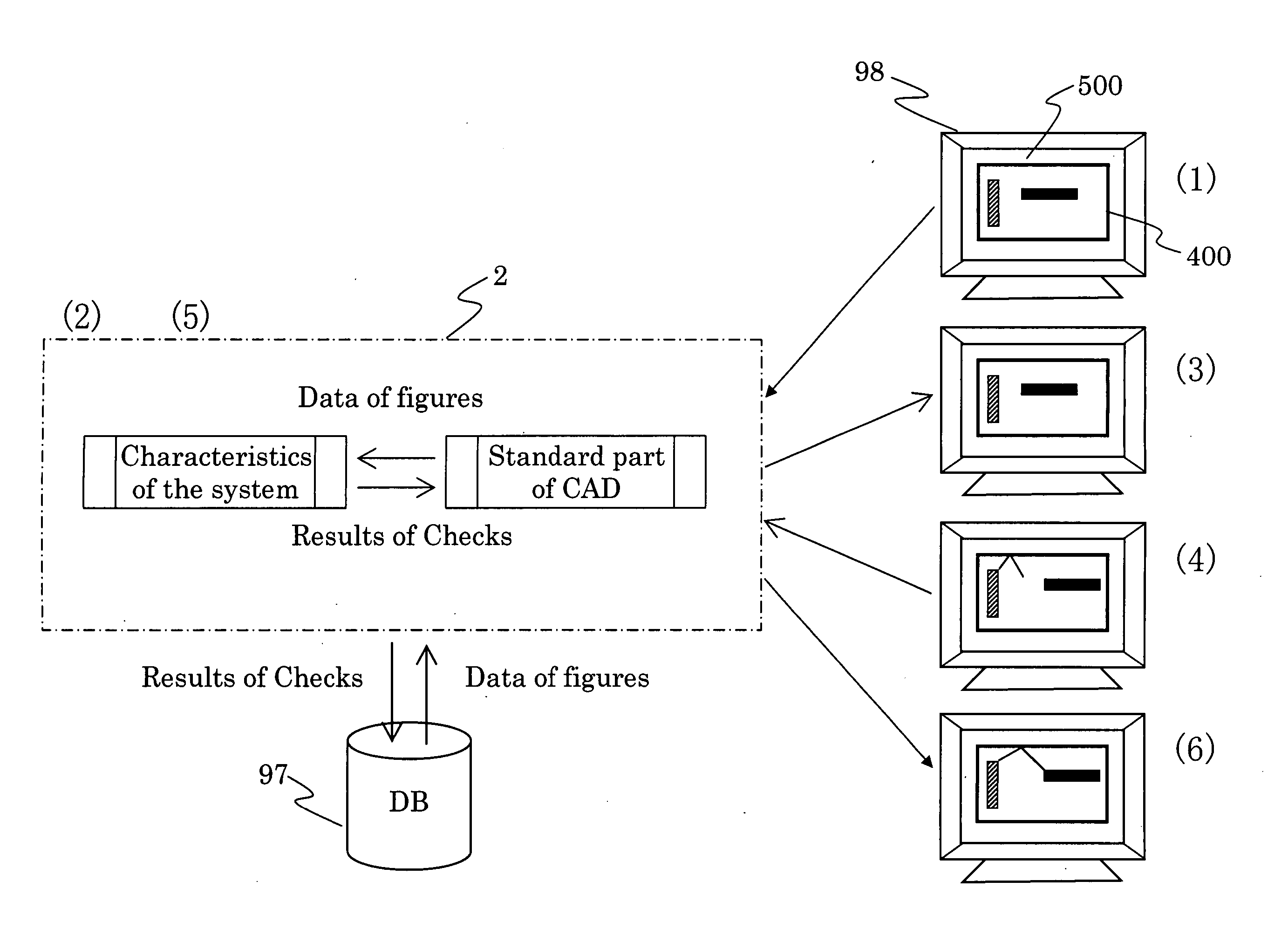
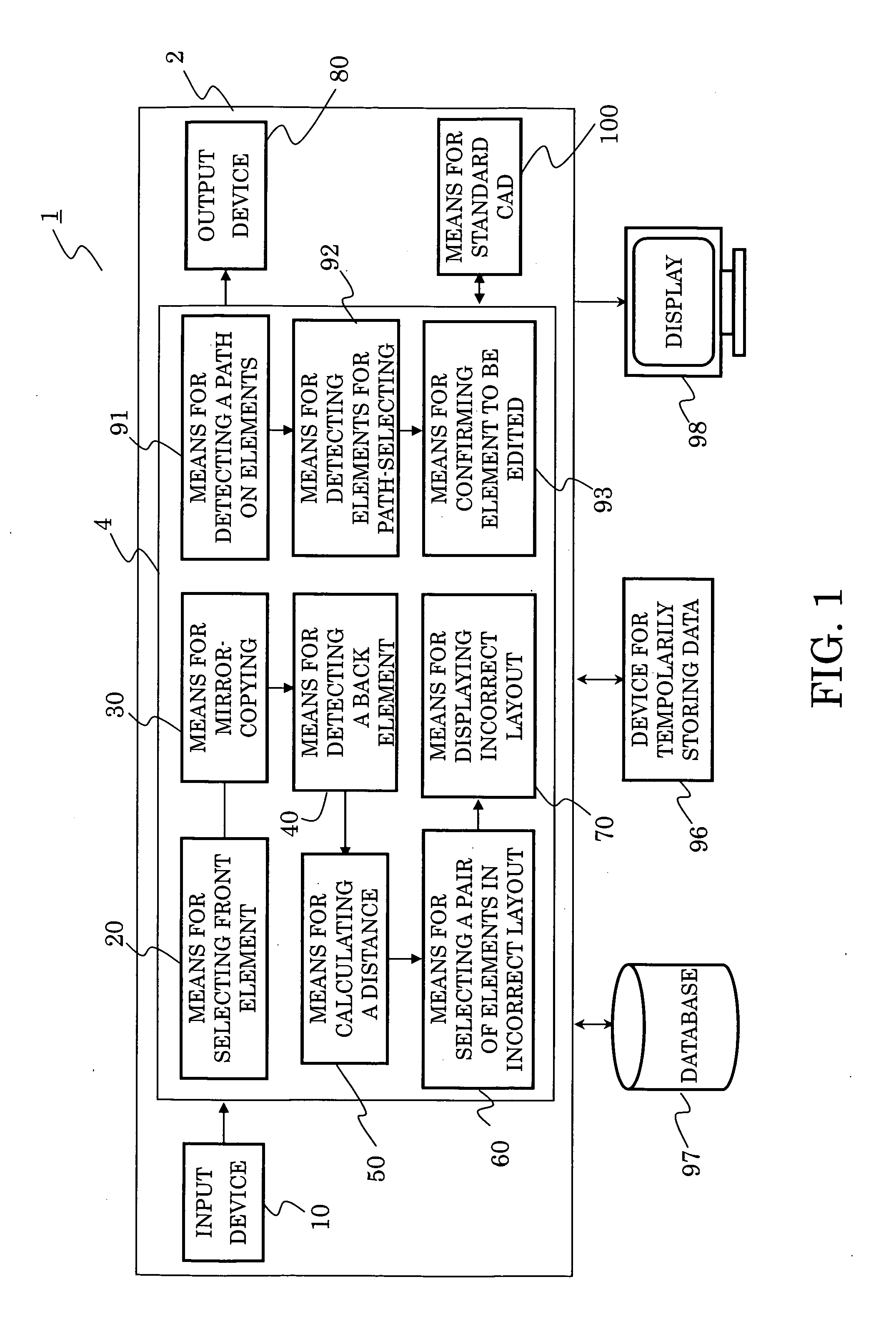
[0041] A preferred embodiment of the present invention is shown in FIG. 1 as a computer-aided design system (CAD system) 1. In FIG. 1, essential parts of the CAD system 1 are shown as a block diagram, and the system 1 may b...


PUM


Abstract

Printed circuit board (PCB) design support apparatus and method are provided. The target element disposed on a front surface of the printed circuit board is mirror-copied, and then the straight line distance between the mirror copied element and a back element disposed on the back surface of the PCB is calculated under the condition that the thickness of the PCB is zero. The resultant creepage distance between the target element and the back element is obtained by adding the thickness of the PCB to the straight line distance. The creepage distance can be obtained accurately and quickly by a calculation on a straight line distance.

Description

BACKGROUND OF THE INVENTION [0001] 1. Field of the Invention [0002] The invention relates to a method for computer aided design, the system therefore and a medium storing the method, more particularly relates to the method, the system, and the medium which provide calculating distances between elements mounted on each surface of a printed circuit board. [0003] 2. Description of the Related Art [0004] A calculation of a distance between elements mounted on each surface of a printed circuit board (PCB), can make it possible to evaluate influences of noise caused by a possible creepage discharge. The distance is measured along the surfaces, the distance is referred to as the creepage distance hereinafter, and the distance should be evaluated whether to agree or not with requirements in specifications and / or standards. [0005] The layout of elements formed or arranged on PCBs is usually designed with a computer aided design system, hereinafter referred to as CAD system. In case of use of...

Claims


Application Information

Patent Timeline
IPC IPC(8): G06F17/50
CPCG06F17/5068G06F30/39G06F9/455
Inventor FUJIMURA, KOUJI
Owner FUJITSU LTD
Features
  • Generate Ideas
  • Intellectual Property
  • Life Sciences
  • Materials
  • Tech Scout
  • Unparalleled Data Quality
  • Higher Quality Content
  • 60% Fewer Hallucinations
Learn More