
Method for recording identification information on semiconductor chip, and imaging device

a technology of identification information and semiconductor chips, applied in semiconductor devices, instruments, computing, etc., can solve the problems of reducing manufacturing efficiency, requiring long time, and image sensor chips cannot be distinguished from each other, and achieve the effect of effective recording

Inactive Publication Date: 2006-12-21
FUJIFILM CORP +1
View PDF7 Cites 20 Cited by
  • Summary
  • Abstract
  • Description
  • Claims
  • Application Information

AI Technical Summary

Benefits of technology

[0009] A main object of the present invention is to provide a method for recording identification information on semiconductor chips, which enables to distinguish each semiconductor chip and to perform effective recording of the identification information,on the semiconductor chip in view of time and space.
[0012] The top surface identification information and the under surface identification information are preferably letters, numerals, symbols or combinations of them, for easy interpretation of the information. Alternatively, the under surface identification information may be plural barcodes arranged in different directions. In this construction, readability of the information is improved when the information is read by a reader such as a barcode reader.
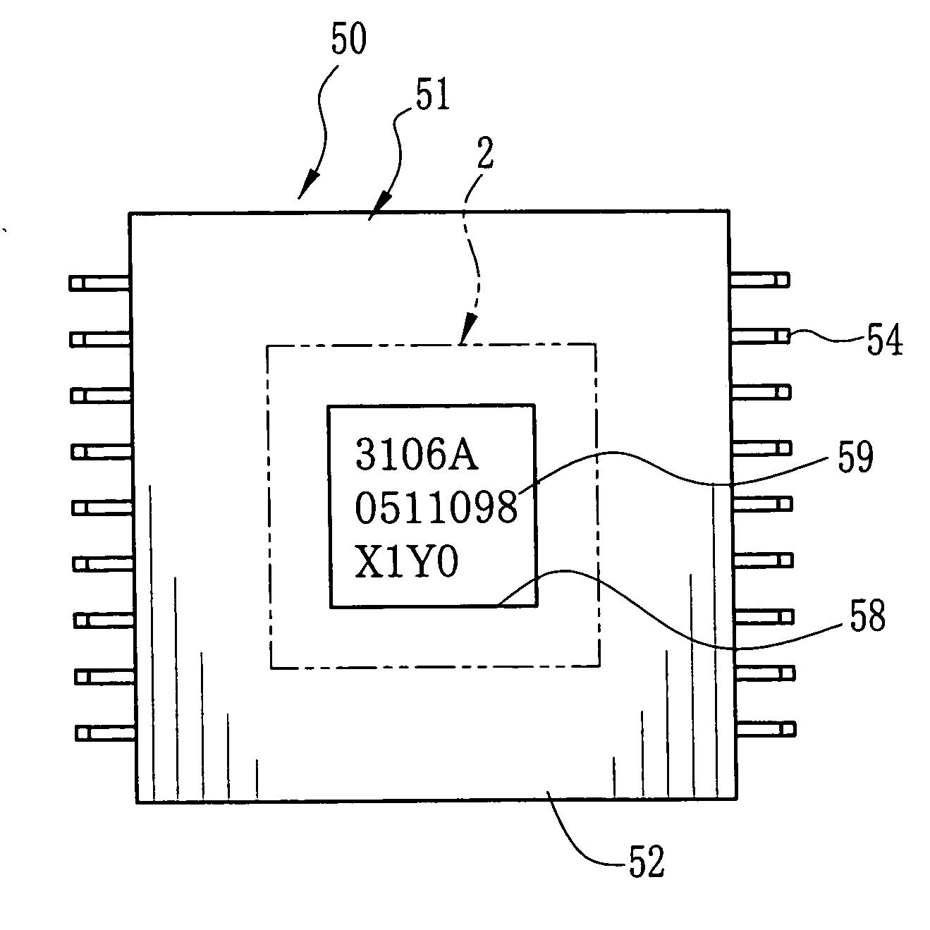
[0013] As a method for recording of the under surface identification information, a laser marking, ink-jet and so on can be used. In the ink-jet method, the ink preferably has heat-resistance and water-resistance, so that the identification information is prevented from being removed by heat in dicing or cooling water.
[0015] An imaging device of the present invention comprises an image sensor chip having a top surface provided with a light receiving section and an under surface provided with identification information, a package body having a chip chamber on a top surface thereof for containing the image sensor chip, an opening penetrating through between an under surface of the package body and a bottom surface of the chip chamber, and a transparent cover for sealing the chip chamber. The identification information on the under surface of the image sensor is visible through the opening. In addition, the opening may be sealed with a transparent sealing plate not to lose the visibility of the identification information.
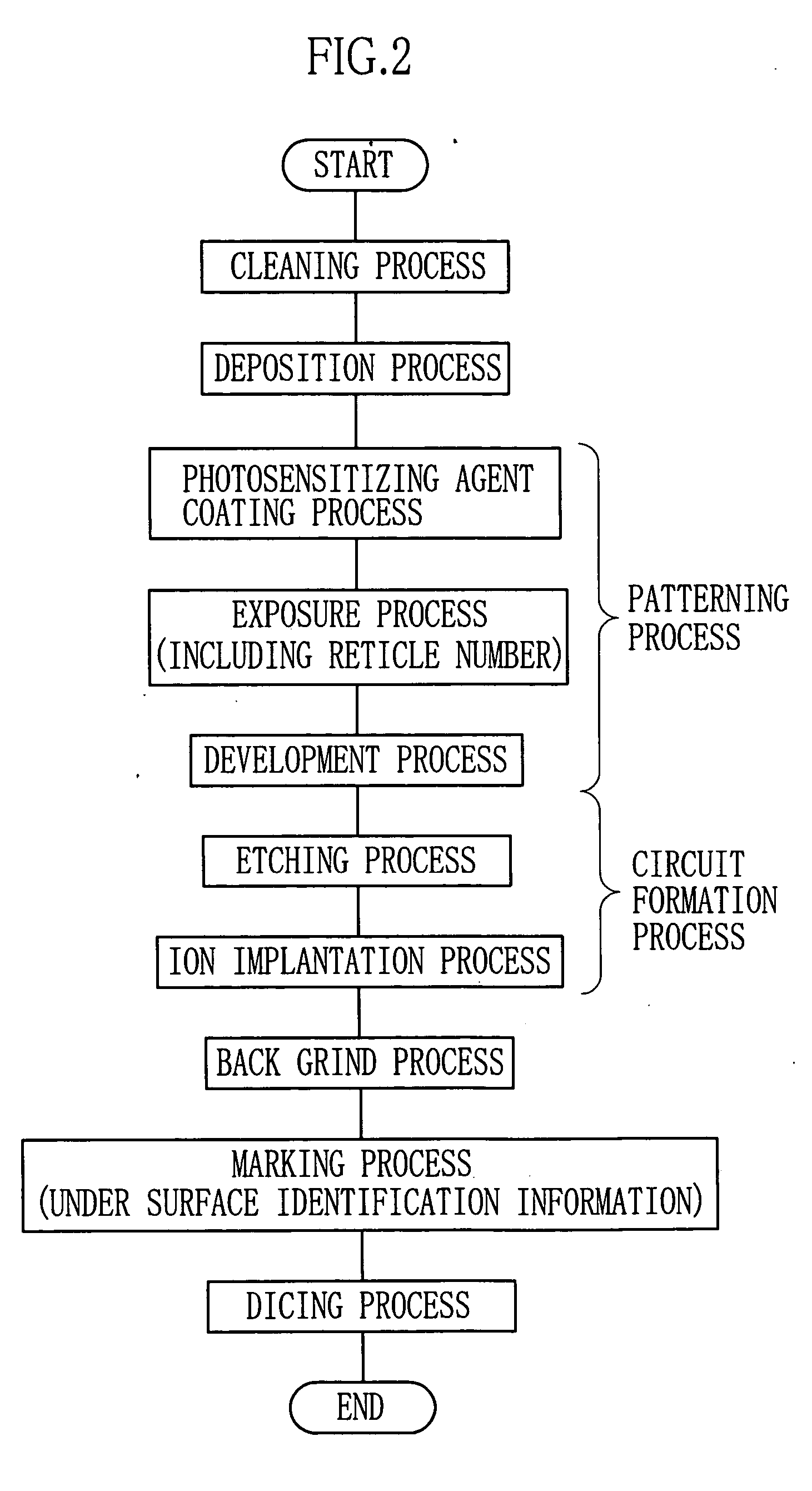
[0016] According to the method for recording identification information on semiconductor chips of the present invention, since the identification information can be recorded both on the top and under surfaces of the wafer, maximum amount of information that can be recorded can be increased. Since the recording on the top surface is performed by exposure through the mask, the identification information and the circuit pattern can be exposed at the same time. Accordingly, a number of manufacturing processes is, not increased. Since the identification information on the under surface of the wafer is recorded on the basis of the shot of exposure on the top surface of the wafer, the time required to record the information can be shortened as compared with recording the identification information chip by chip. In addition, since each of the semiconductor chips can be distinguished from each other on a single shot basis and a single reticle basis by referring the identification information recorded on the top and under surfaces thereof, distinction of the semiconductor chip can be improved. In this configuration, the recording of the identification information on the semiconductor chip is carried out effectively in view of time and space, and the cost for manufacturing the semiconductor chips is not increased.
[0017] According to the imaging device of the present invention, since the identification information recorded on the image sensor chip is visible in the hollow package, number of items of identification information recorded on an outer surface of the package body can be reduced, or the identification information on the package body can be omitted.

Problems solved by technology

Specifically, since only position information of circuit patterns (image sensor chips) exposed in a single shot can be recorded with this method, the image sensor chips cannot be distinguished from each other.
In the method of Japanese Patent Laid-Open Publication No. 04-106960, there is a problem that recording detailed identification information to each chip by the laser marking or the like requires long time, which reduces efficiency of manufacturing.
In addition, there is further problem that the identification information recorded on the under surface of the chip is invisible after the image sensor chip is contained in the hollow package.

Method used


Image

  • Method for recording identification information on semiconductor chip, and imaging device
  • Method for recording identification information on semiconductor chip, and imaging device
  • Method for recording identification information on semiconductor chip, and imaging device

Examples


Embodiment Construction

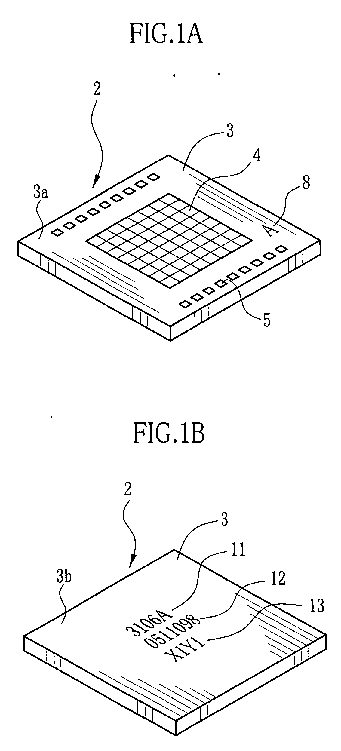
[0031] As shown in FIG. 1A and FIG. 1B, in an image sensor chip 2 which is for example a CCD ship, a light receiving section 4 and a plurality of input / output pads 5 are formed on a top surface 3a of a chip substrate 3 made of silicon or the like. In the light receiving section 4, plural photodiodes (PD) are arranged in a matrix, and color filters and microlenses are provided above the photodiodes. The input / output pads 5 are formed of a conductive metal, and electrically connected to the light receiving section 4.

[0032] On the top surface 3a of the chip substrate 3 and lateral to the light receiving section 4, a reticle number 8 as identification information is provided. The reticle number 8 represents a position of a reticle on a mask used for forming circuit patterns on a wafer through exposure.

[0033] On an under surface 3b of the chip substrate 3, a product code 11, a manufacture code 12, and a shot position code 13 are recorded as identification information. The product code ...


PUM


Abstract

On a wafer coated with photosensitizing agent, plural shots of exposure are applied through a mask including a plurality of reticles each of which has a circuit pattern and a top surface identification information, while the mask and the wafer are relatively moved. Then the wafer is developed and etched to form convex or concave reticle numbers (top surface identification information) on a metal layer which is the uppermost part or a part close to the uppermost part of the wafer. The reticle numbers enables to distinguish each of reticles on the mask. Next, an under surface identification information is recorded on an under surface of the wafer by laser marking or another method. The under surface identification information enables to distinguish each of the shots of exposure.

Description

BACKGROUND OF THE INVENTION [0001] 1. Field of the Invention [0002] The present invention relates to a method for recording identification information on a semiconductor chip, and relates to an imaging device which packages an image sensor chip having the recorded identification information. [0003] 2. Description Related to the Prior Art [0004] In many semiconductor devices, a semiconductor chip is contained in a package, and input / output pads of the semiconductor chip are connected to leads of the package through bonding wires. A hollow package is known as one of the package. [0005] The hollow package comprises a box-like package body formed of a ceramic or a plastic and having a chip chamber of recessed-shape on a top surface thereof, leads provided in the package body by insert molding, and a cover attached on the top surface of the package body to seal the chip chamber. Recently, bumps are often used instead of the bonding wires to connect between the semiconductor chip and the ...

Claims


Application Information

Patent Timeline
Patent Type & Authority Applications(United States)
IPC IPC(8): G06K19/06
CPCH01L23/544H01L27/14618H01L2223/54406H01L2223/54413H01L2223/54433H01L2223/5448H01L24/48H01L2224/48247H01L2924/01046H01L2924/16195H01L2224/48091H01L2924/00014H01L2224/05554H01L2924/10162H01L2224/45099H01L2224/45015H01L2924/207
Inventor MISAWA, TAKESHISAITO, MAKI
Owner FUJIFILM CORP
Learn More