Pixel circuit with low noise in image sensor

a technology of image sensor and circuit, applied in the field of image sensor, can solve the problems of picture quality deterioration and increased noise in the global shutter operation, and achieve the effect of preserving picture quality and reducing nois

Active Publication Date: 2006-12-21
SAMSUNG ELECTRONICS CO LTD
View PDF4 Cites 52 Cited by
  • Summary
  • Abstract
  • Description
  • Claims
  • Application Information

AI Technical Summary

Benefits of technology

[0026] The present invention may be used to particular advantage when the image sensor is a CMOS (complementary metal oxide semiconductor) image sensor. However, the present invention may also be advantageously applied for other types of image sensors.
[0027] In this manner, the reset signal is generated immediately before the image signal for reduced noise in

Problems solved by technology

Rather, a reset signal VRES may be sampled after the image signal VSIG is sampled, which results in increased noise in the

Method used


Image

  • Pixel circuit with low noise in image sensor
  • Pixel circuit with low noise in image sensor
  • Pixel circuit with low noise in image sensor

Examples


Embodiment Construction

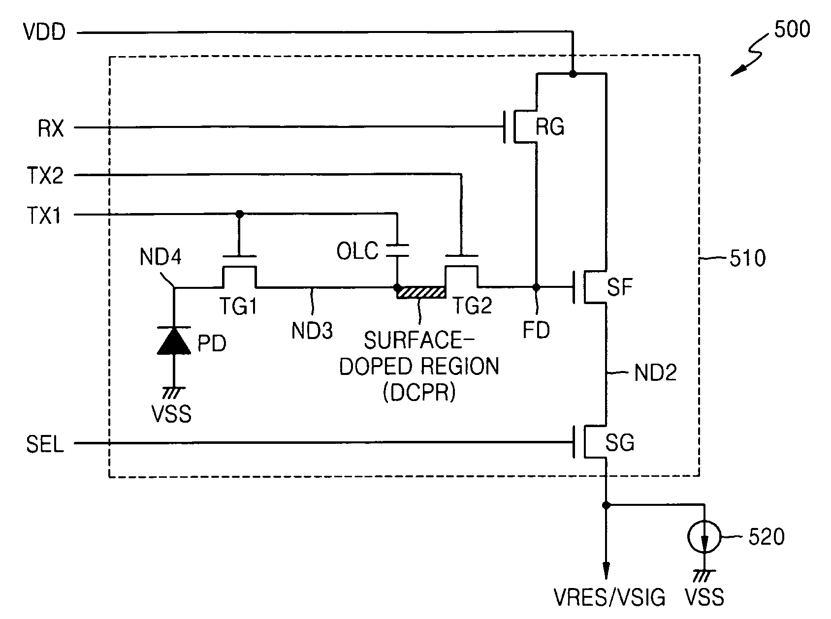
[0039]FIG. 5 is a circuit diagram of a pixel driving circuit 500 of a CMOS (complementary metal oxide semiconductor) image sensor 600 in FIG. 9, according to an embodiment of the present invention. Referring to FIG. 5, the pixel driving circuit 500 includes a pixel circuit 510 and a bias circuit 520 for biasing an output node generating a reset signal VRES and an image signal VSIG.

[0040] Referring to FIGS. 5 and 9, the CMOS image sensor 600 includes an APS (active pixel sensor) array 602 of a plurality of pixel circuits. FIG. 9 shows a first pixel circuit 604, a second pixel circuit 606, a third pixel circuit 608, and a fourth pixel circuit 610. Four pixel circuits are illustrated in FIG. 9, but a typical CMOS image sensor has more numerous pixel circuits for high resolution of the image sensor.

[0041] Each of the pixel circuits 604, 606, 608, and 610 in the APS array 602 is implemented similarly to the pixel circuit 510 of FIG. 5. In addition, a column of pixel circuits is coupled...


PUM


Abstract

A pixel circuit of an image sensor includes a photo-converting unit such as a photo-diode for generating charge from incident light. The pixel circuit also includes a charge storing capacitor for storing the charge generated by the photo-converting unit. The pixel circuit further includes a floating diffusion node that receives the charge from the charge storing unit after being reset. Thus, an image signal VSIG is generated after a reset signal VRES is generated from the pixel circuit.

Description

BACKGROUND OF THE INVENTION [0001] This application claims priority to Korean Patent Application No. 2005-53017, filed on Jun. 20, 2005 in the Korean Intellectual Property Office, the disclosure of which is incorporated herein in its entirety by reference. [0002] 1. Field of the Invention [0003] The present invention relates generally to image sensors, and more particularly, to a pixel circuit with low noise for a global shutter operation in a CMOS image sensor. [0004] 2. Description of the Related Art [0005] A CMOS image sensor (CIS) in a cellular phone camera, a digital still camera, etc., converts images into electrical signals, and converts the electrical signals into digital signals. A digital image signal output from the CMOS image sensor is color (Red, Green, or Blue) image data. The digital image signal is further processed for driving a display, such as a LCD. [0006]FIG. 1 is a block diagram of a conventional CMOS image sensor 100. Referring to FIG. 1, the image sensor 100 ...

Claims


Application Information

Patent Timeline
IPC IPC(8): H01L31/00H01L27/00
CPCH04N5/361H01L27/14609H04N25/63H04N25/76
Inventor ASABA, TETSUO
Owner SAMSUNG ELECTRONICS CO LTD
Why Eureka
Try Eureka