Wide dynamic range sensor having a pinned diode with multiple pinned voltages

a diode and wide dynamic range technology, applied in the field of photodiodes, can solve the problems of incident light captured and converted into charge during the integration period being greater than the capacity of the photosensor, and the dynamic range is limited on the upper end, so as to achieve low fixed pattern noise, control the effect of photosensors and anti-blooming leakag

Active Publication Date: 2006-12-21
APTINA IMAGING CORP
View PDF12 Cites 15 Cited by
  • Summary
  • Abstract
  • Description
  • Claims
  • Application Information

AI Technical Summary

Benefits of technology

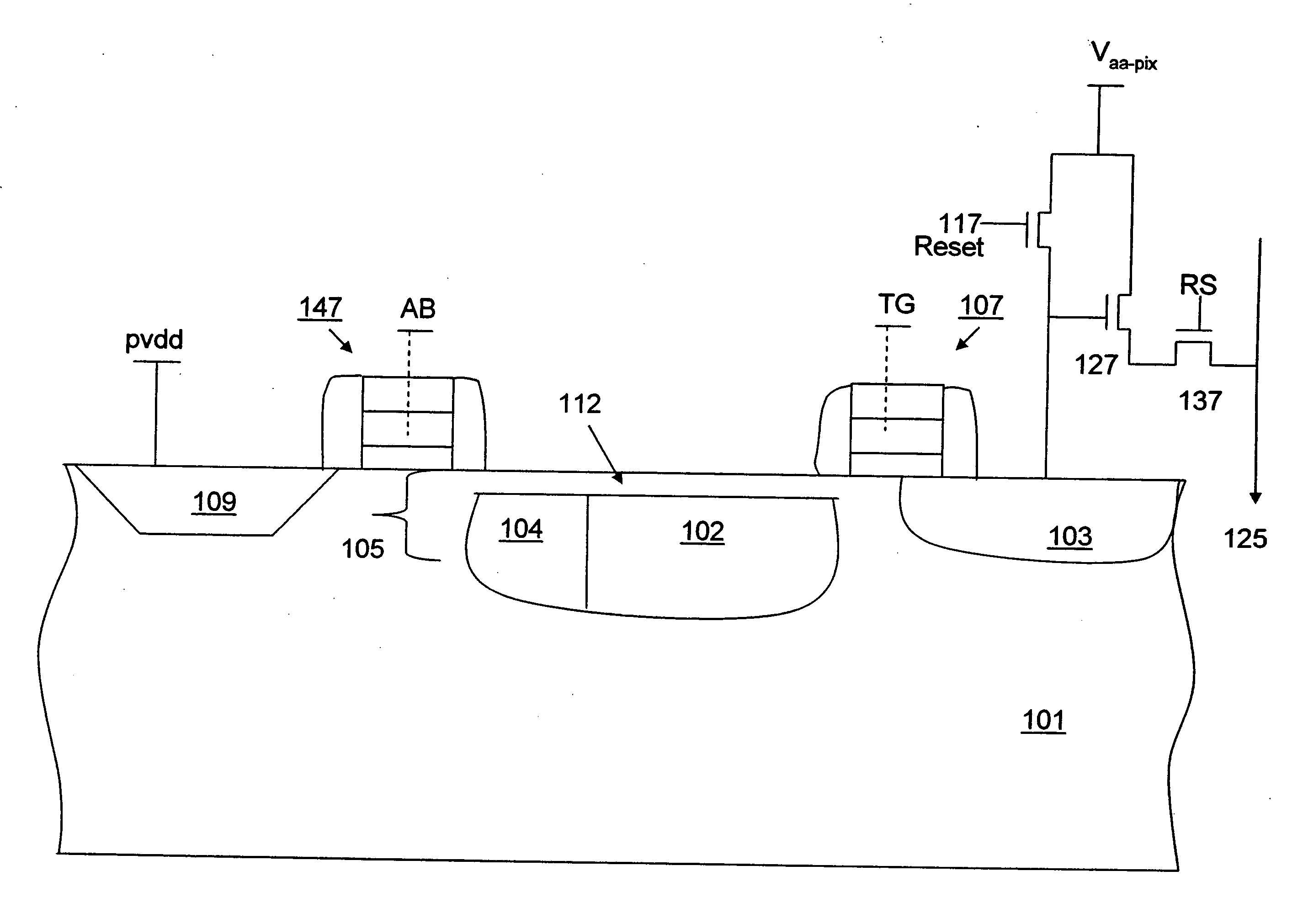
[0020] Exemplary embodiments of the invention provide a pixel cell having a high dynamic range with low fixed pattern noise. The pixel cell has controlled photosensor anti-blooming leakage by having dual pinned voltage regions, one of which is be used to set the anti-blooming characteristics of the photosensor. Additional exemplary embodiments also employ an anti-blooming transistor in conjunction with the dual pinned photosensor.

Problems solved by technology

The dynamic range is limited on an upper end by the charge saturation level of the sensor, and on a lower end by noise imposed limitations and / or quantization limits of the analog-to-digital converter used to produce the digital image.
When the dynamic range of an image sensor is too small to accommodate the variations in light intensities of the imaged scene, e.g. by having a low saturation level, image distortion occurs.
Another problem associated with charge generation in conventional pixel cells occurs when the incident light captured and converted into charge during an integration period is greater than the capacity of the photosensor.
A pixel cell's maximum charge capacity Qs may be reached at a relatively low level of illumination, which causes the pixel cell to be easily saturated, thereby limiting the dynamic range of the pixel.
Often times this leakage causes charges to migrate to adjacent pixel cells causing cross-talk.
The residual charge may cause the photosensor to exceed its maximum capacity, thereby causing excess charge to overflow to adjacent pixels.
This undesirable phenomenon is known as blooming and results in a number of vertical and / or horizontal streaks in the resultant output image.
The drawback associated with the FIG. 3 cell 50, is that CMOS transistors have a high deviation in threshold voltage Vth from wafer to wafer, and often from transistor to transistor.
For example, the gate oxide layer can assimilate floating charges that make it difficult to precisely control operating transistor characteristics.
This deviation leads to an uncertainty in the amount of charge stored from pixel cell to pixel cell since the threshold voltage Vth of each transistor, including the anti-blooming transistor, could vary.
The variance of charge storage from pixel cell to pixel cell leads to fixed pattern noise (FPN) in an imager array resulting in diminished image quality because of the non-uniformity of barrier heights between pixels.

Method used


Image

  • Wide dynamic range sensor having a pinned diode with multiple pinned voltages
  • Wide dynamic range sensor having a pinned diode with multiple pinned voltages
  • Wide dynamic range sensor having a pinned diode with multiple pinned voltages

Examples


Embodiment Construction

[0041] In the following detailed description, reference is made to the accompanying drawings which form a part hereof, and in which is shown by way of illustration specific embodiments in which the invention may be practiced. These embodiments are described in sufficient detail to enable those skilled in the art to practice the invention, and it is to be understood that other embodiments may be utilized, and that structural, logical and electrical changes may be made without departing from the spirit and scope of the present invention.

[0042] The term “substrate” is to be understood as a semiconductor-based material including silicon, silicon-on-insulator (SOI) or silicon-on-sapphire (SOS) technology, doped and undoped semiconductors, epitaxial layers of silicon supported by a base semiconductor foundation, and other semiconductor structures. Furthermore, when reference is made to a “substrate” in the following description, previous process steps may have been utilized to form regio...


PUM


Abstract

A pixel cell has controlled photosensor anti-blooming leakage by having dual pinned voltage regions, one of which is used to set the anti-blooming characteristics of the photosensor. Additional exemplary embodiments also employ an anti-blooming transistor in conjunction with the dual pinned photosensor. Other exemplary embodiments provide a pixel with two pinned voltage regions and two anti-blooming transistors. Methods of fabricating the exemplary pixel cells are also disclosed.

Description

CROSS-REFERENCE TO RELATED APPLICATION [0001] This application is a divisional of U.S. patent application Ser. No. 10 / 921,226, filed on Aug. 19, 2004, the subject matter of which is incorporated in its entirety by reference herein.FIELD OF THE INVENTION [0002] The present invention relates to the field of semiconductor devices and, in particular, to a photodiode for improving the dynamic range and fixed pattern noise characteristics of a pixel sensor cell. BACKGROUND OF THE INVENTION [0003] A CMOS imager includes a focal plane array of pixel cells, each cell includes a photosensor, for example, a photogate, photoconductor or a photodiode overlying a substrate for producing a photo-generated charge in a doped region of the substrate. In a CMOS imager, the active elements of a pixel cell, for example a four transistor pixel, perform the necessary functions of (1) photon to charge conversion; (2) transfer of charge to the floating diffusion region; (3) resetting the floating diffusion ...

Claims


Application Information

Patent Timeline
Patent Type & Authority Applications(United States)
IPC IPC(8): H01L31/113
CPCH01L27/14603H01L27/14689H01L27/14654H01L27/14609
Inventor HONG, SUNGKWON C.KRYMSKI, ALEX
Owner APTINA IMAGING CORP
Why Eureka
Try Eureka