Method circuit and system for compensating for temperature induced margin loss in non-volatile memory cells

Active Publication Date: 2006-12-21
SAIFUN SEMICON
View PDF99 Cites 56 Cited by
  • Summary
  • Abstract
  • Description
  • Claims
  • Application Information

AI Technical Summary

Benefits of technology

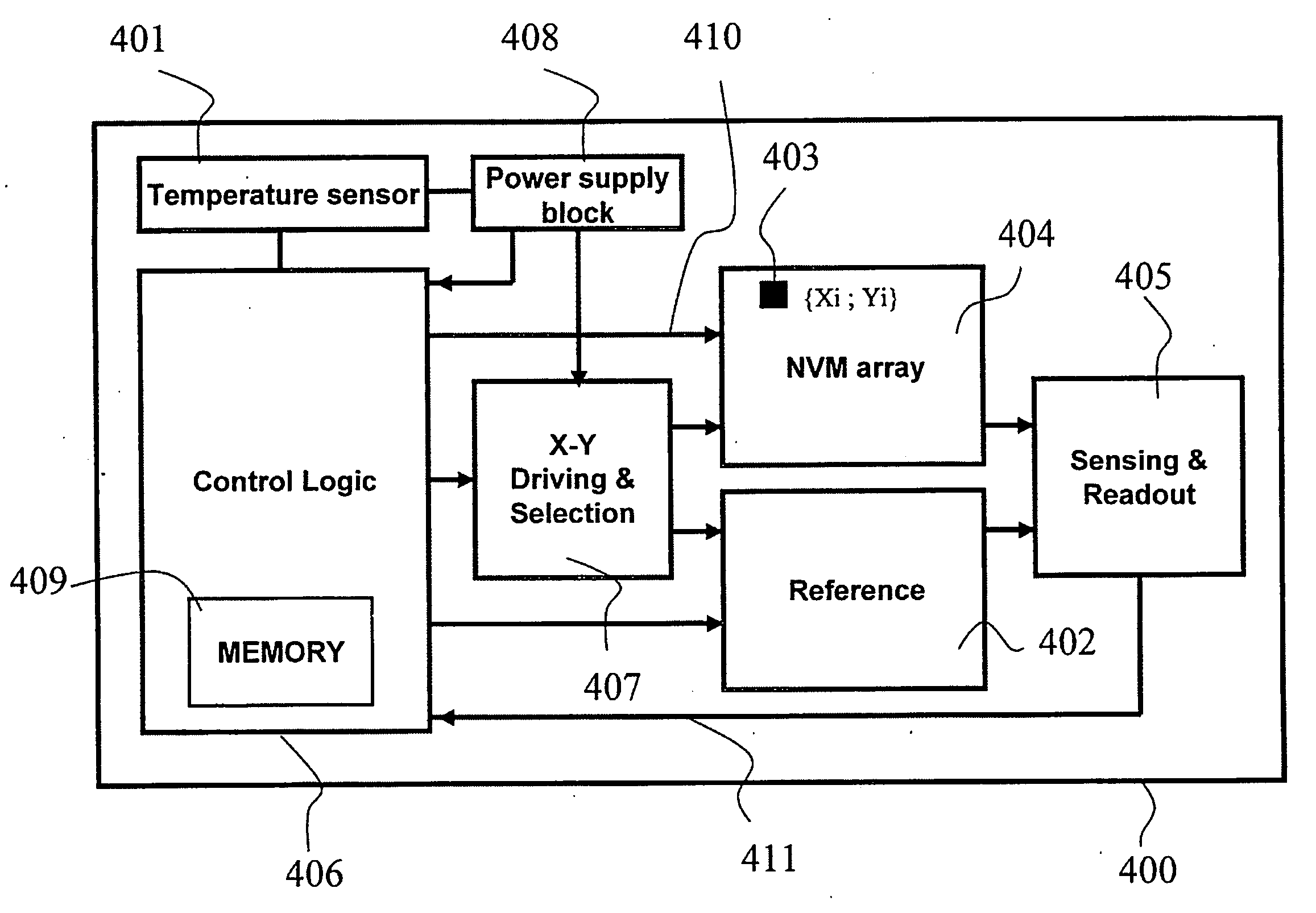
[0028] In some preferred embodiments of the present invention, a reference cell for a program verify operation is selected such that its volt threshold (“VT”) is higher as the temperature of the NVM cell increases

Problems solved by technology

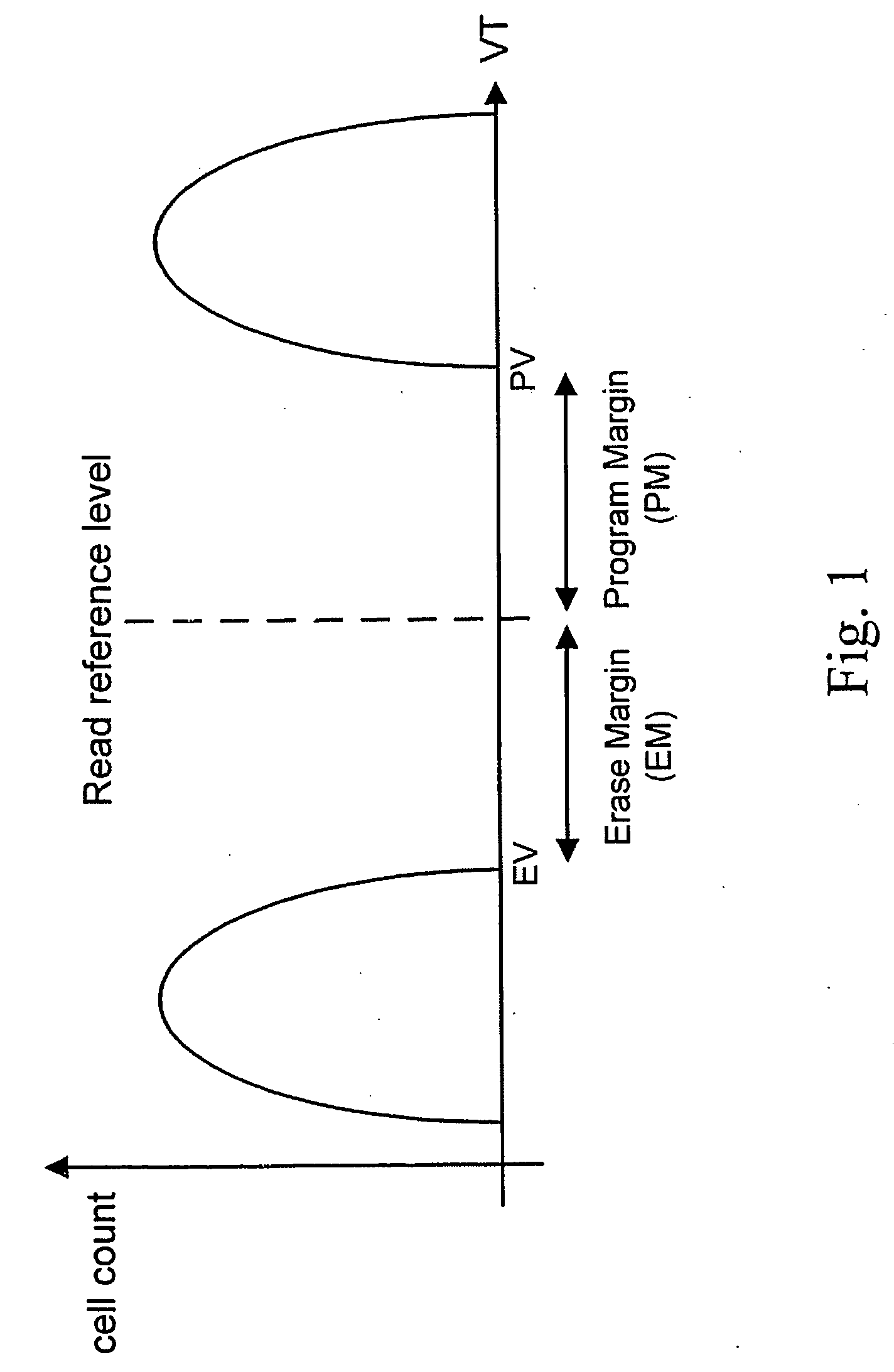
However, as is well known the program and erase margins may detrimentally vary due to any one or several factors, including but not limited to charge leakage from the cell's charge storage region, temperature changes, and due to interference from the operation of neighboring NVM cells.
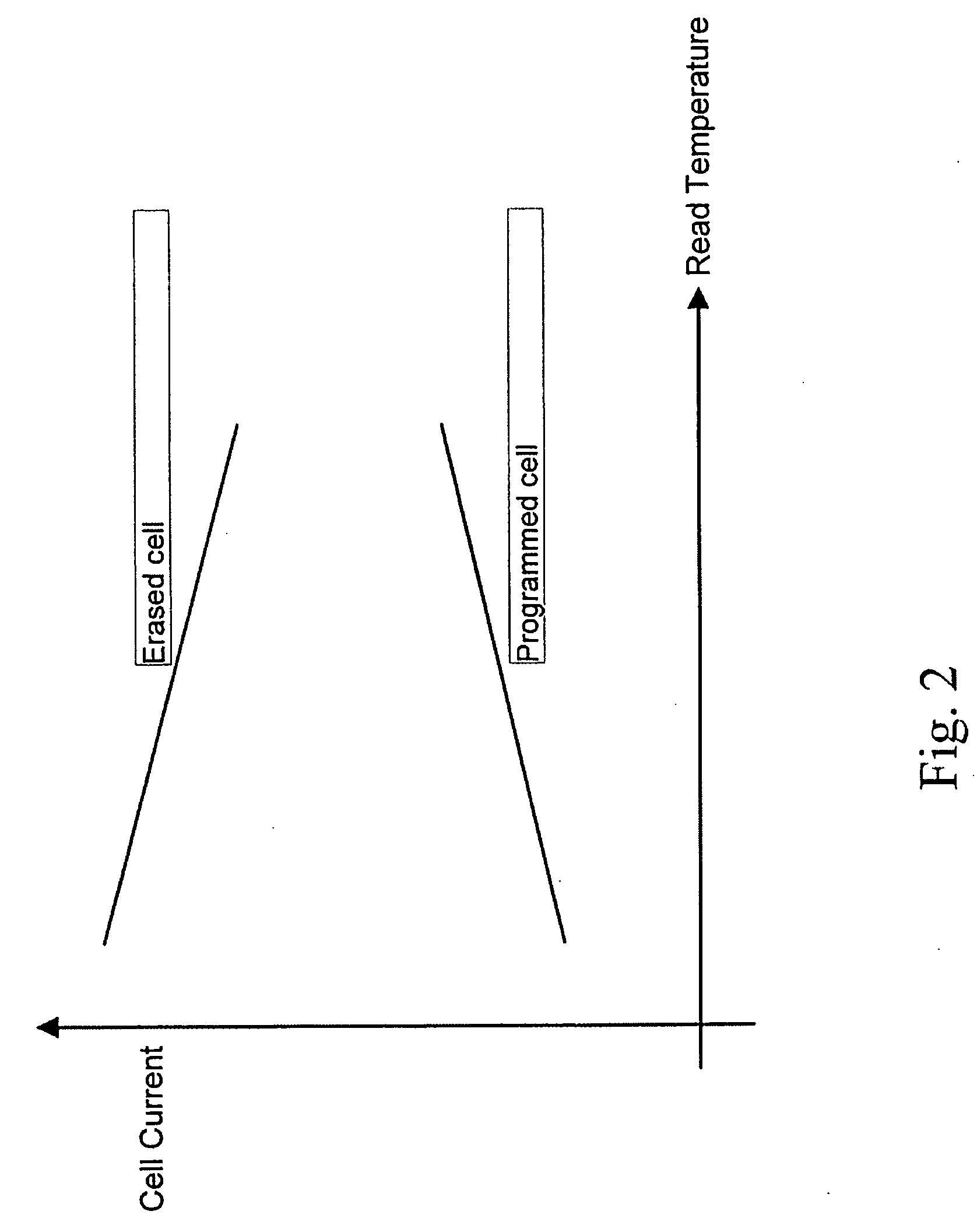
Among the various factors, temperature deviations a cell may experience between the time it is programmed and read may result in deviations up to several hundreds of millivolts in the threshold voltage of a memory cell, which may detrimentally affect these margins.
Being fabricated substantially under the same manufacturing conditions, NVM cells and reference cells, which typically reside on the same substrate, initially have similar temperature coefficients, resulting in both of them being potentially equally affected by temperature deviations within the operating temperature range.
In general, the more programming/erasing cycles a NVM cell undergoes, the greater the divergence becomes, until, at some certain point, the margins become detrimentally affec

Method used


Image

  • Method circuit and system for compensating for temperature induced margin loss in non-volatile memory cells
  • Method circuit and system for compensating for temperature induced margin loss in non-volatile memory cells
  • Method circuit and system for compensating for temperature induced margin loss in non-volatile memory cells

Examples


Embodiment Construction

[0045] In the following detailed description, numerous specific details are set forth in order to provide a thorough understanding of the invention. However, it will be understood by those skilled in the art that the present invention may be practiced without these specific details. In other instances, well-known methods, procedures, components and circuits have not been described in detail so as not to obscure the present invention.

[0046] Unless specifically stated otherwise, as apparent from the following discussions, it is appreciated that throughout the specification discussions utilizing terms such as “processing”, “computing”, “calculating”, “determining”, or the like, refer to the action and / or processes of a computer or computing system, or similar electronic computing device, that manipulate and / or transform data represented as physical, such as electronic, quantities within the computing system's registers and / or memories into other data similarly represented as physical ...


PUM


Abstract

The present invention consists of a method and system for compensating, over time and over an operating temperature range, for margin loss in a non-volatile memory (“NVM”) cell, which method comprises selection of a reference level based on temperature readings obtained from a temperature sensing element that is thermally coupled, directly or indirectly, to the NVM cell. The reference level may be selected from a group consisting of references levels of various types, or it may be obtained by adjusting the output of a single reference based on the temperature reading(s), or it may be obtained by utilizing pre-stored conversion data, which conversion data associates a given temperature reading with a corresponding temperature range that is, in turn, associated with a corresponding reference level. A pool of likewise reference cells may be provided, and the reference level may be selected from this pool, based on its association to the temperature reading. The pool of reference cells may consist of Program verify reference cells, or Erase verify reference cells.

Description

FIELD OF THE INVENTION [0001] The present invention relates generally to the field of non-volatile memory cells. More particularly, the present invention relates to a method, circuit and system for compensating over time for margin loss in non-volatile memory (“NVM”) cells over an operating temperature range. BACKGROUND OF THE INVENTION [0002] NVM cells are generally operated (e.g. programmed, read, and erased) using one or more reference cells and / or structures. In order to determine a condition or state of a memory cell being operated, the cell's operating characteristics may be compared against a reference memory cell or structure usually operated under similar conditions as the cell of interest. As is well known, an NVM cell's state may be defined and determined by its threshold voltage, the voltage at which the cell begins to conduct current. A NVM cell's threshold voltage level is typically correlated to the amount of charge stored in a charge storage region of the cell. Diffe...

Claims


Application Information

Patent Timeline
IPC IPC(8): G11C11/34
CPCG11C16/3404G11C16/3459G11C16/3445
Inventor BETSER, YORAMSOFER, YAIRMAAYAN, EDUARDO
Owner SAIFUN SEMICON
Why Eureka
Try Eureka