Double-sided wiring board, double sided wiring board manufacturing method, and multilayer wiring board

a wiring board and manufacturing method technology, applied in the field of double-sided wiring boards, can solve the problems of increased cost, unsuitable for high-frequency electricity use, and problems such as wiring density and wiring arrangemen

Inactive Publication Date: 2006-12-28
DAI NIPPON PRINTING CO LTD
View PDF7 Cites 88 Cited by
  • Summary
  • Abstract
  • Description
  • Claims
  • Application Information

AI Technical Summary

Benefits of technology

[0028] The present invention has been made to solve those problems and it is therefore an object of the present invention to provide a wiring board for an IC package, suitable for high-density packaging, and capable of being produced at a productivity higher than that at which the conventional buildup multilayer wiring board can be produced and of solving problems attributable to high-frequency power loss.

Problems solved by technology

However, the fabrication of this buildup multilayer wiring board needs many processes, which directly increase the cost.
The wiring board as shown in FIG. 8 suffers from large power loss caused by the through holes and hence is unsuitable for uses that deal with high-frequency electricity.
Problems arise in wiring density and wiring arrangement when the core substrate formed by the conventional subtractive process is applied directly to a wiring board for a semiconductor IC package.
However, fabrication of such a buildup multilayer wiring board requires many complicated processes and large cost, and is unsuitable for uses that deal with high-frequency electricity because the through holes cause large power loss.

Method used


Image

  • Double-sided wiring board, double sided wiring board manufacturing method, and multilayer wiring board
  • Double-sided wiring board, double sided wiring board manufacturing method, and multilayer wiring board
  • Double-sided wiring board, double sided wiring board manufacturing method, and multilayer wiring board

Examples


first embodiment

[0152] A first embodiment of the present invention will be described with reference to the accompanying drawings.

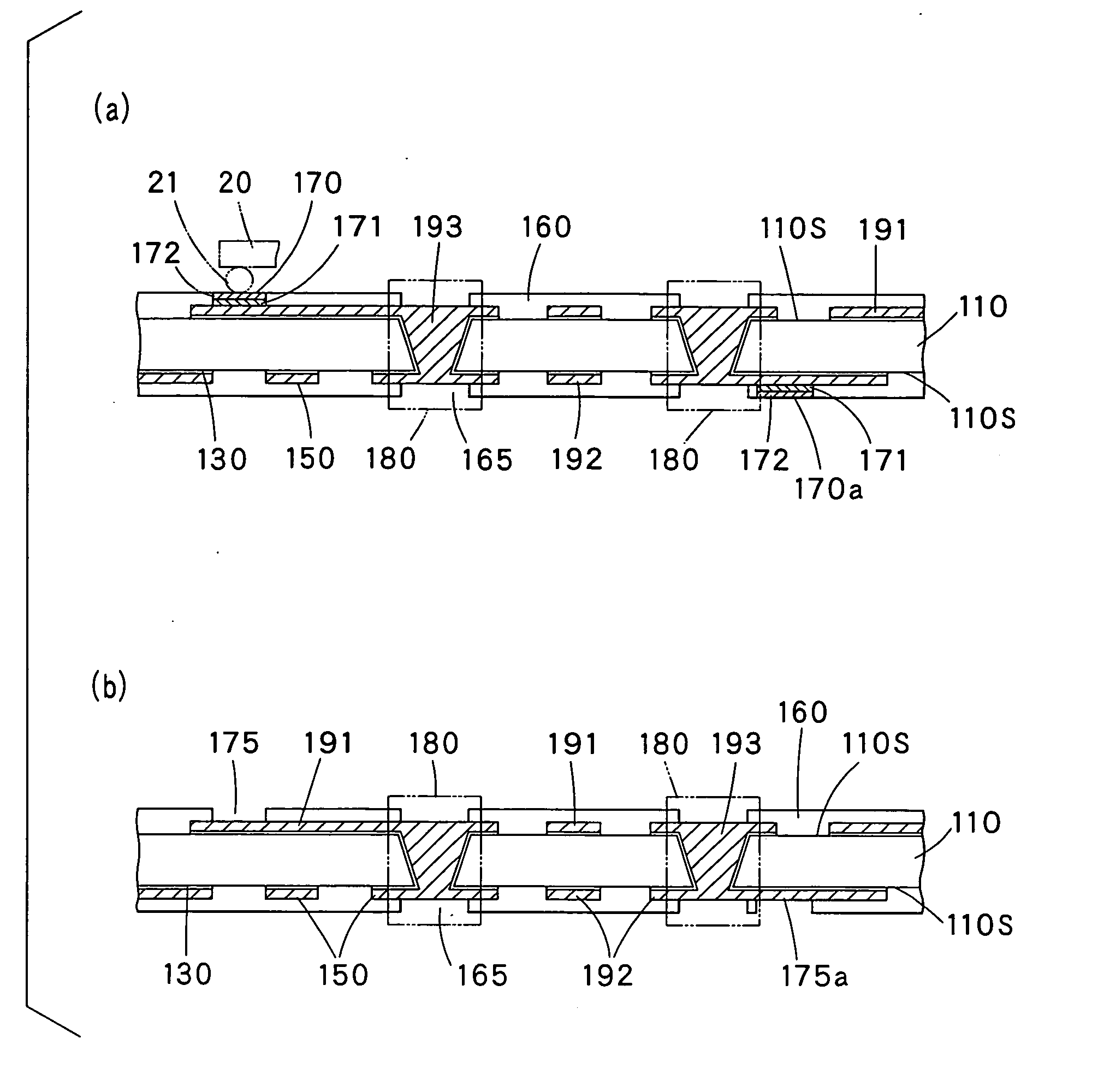
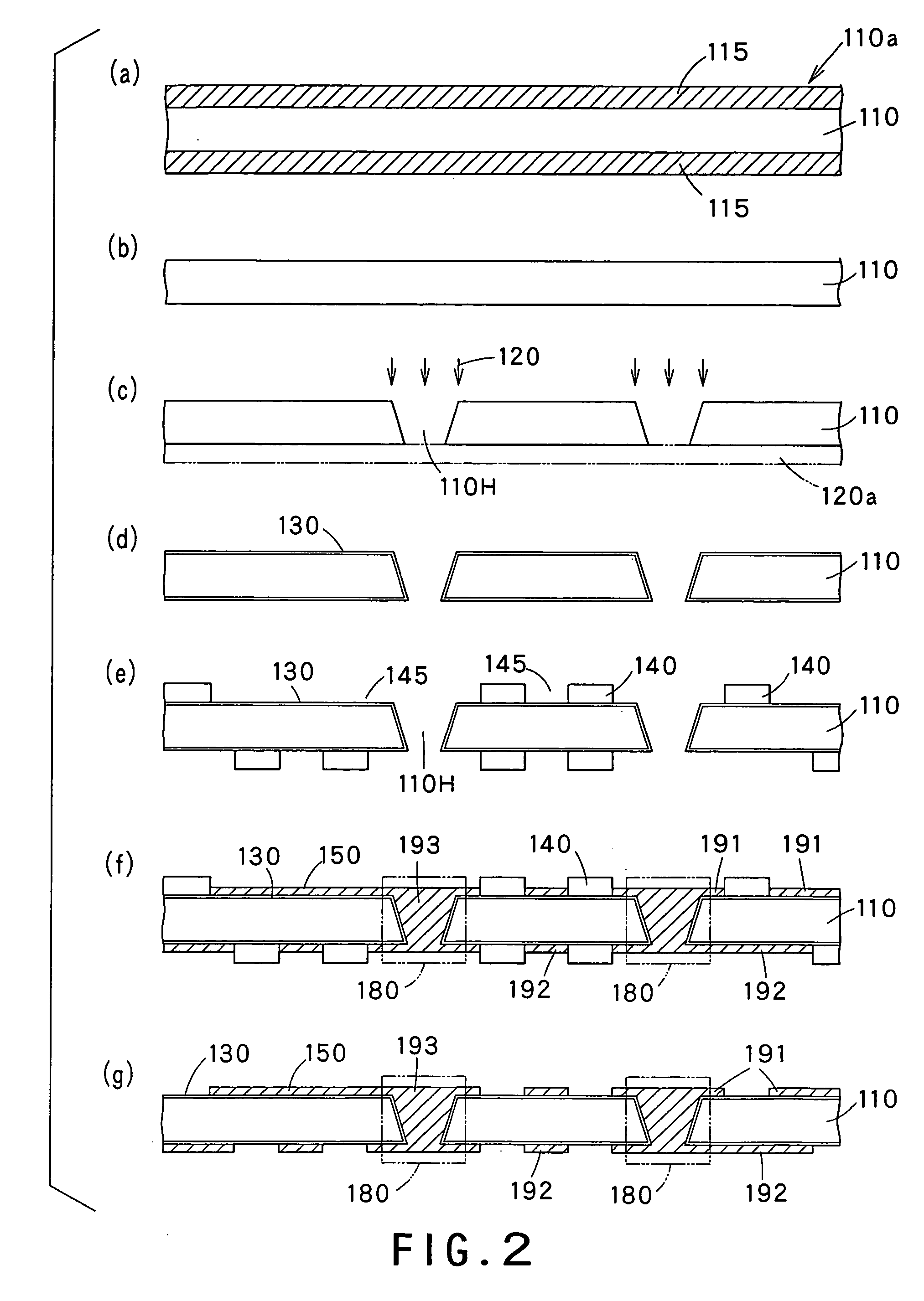
[0153]FIG. 1(a) is a fragmentary sectional view of a double-sided wiring board in a first embodiment according to the present invention, FIG. 1(b) is a double-sided wiring board in a modification of the first embodiment shown in FIG. 1(a), FIGS. 2(a)-2(g) are sectional views of assistance in explaining steps of a double-sided wiring board fabricating method of fabricating the double-sided wiring board in the first embodiment shown in FIG. 1(a), FIGS. 3(a)-3(d) are sectional views of assistance in explaining steps subsequent to those shown in FIGS. 2(a)-2(g), FIGS. 4(a)-4(f) are sectional views of assistance in explaining steps of a double-sided wiring board fabricating method of fabricating a double-sided wiring board in a comparative example, FIGS. 5(a)-5(g) are sectional views of assistance in explaining steps subsequent to those shown in FIGS. 4(a)-4(f), FIGS. 6(a)-6(...

second embodiment

[0227] A second embodiment of the present invention will be described in connection with the accompanying drawings.

[0228]FIG. 11(a) is a fragmentary sectional view of a double-sided wiring board in a second embodiment according to the present invention, FIG. 11(b) is a fragmentary sectional view of a double-sided wiring board in a modification of the second embodiment shown in FIG. 11(a), FIGS. 12(a)-12(g) are sectional views of assistance in explaining steps of a double-sided wiring board fabricating method of fabricating the double-sided wiring board in the second embodiment shown in FIG. 11(a), FIGS. 13(a)-13(d) are sectional views of assistance in explaining steps subsequent to those shown in FIGS. 12(a)-12(g), FIGS. 14(a)-14(f) are sectional views of assistance in explaining steps of a double-sided wiring board fabricating method of fabricating a double-sided wiring board in a comparative example, and FIGS. 15(a)-15(d) are sectional views of assistance in explaining steps subs...


PUM

PropertyMeasurementUnit
height irregularity Rzaaaaaaaaaa
diameteraaaaaaaaaa
diameteraaaaaaaaaa

Abstract

A single wiring layer is formed on each of both the roughened surfaces of a core substrate by a semiadditive method. The wiring layers formed on the surfaces of the core substrate are electrically connected through a through hole formed in the core substrate. The through hole is formed in the core substrate by laser machining. The through hole is filled up with conductive a plug. Both the surfaces of the core substrate are coated with solder resist layers, respectively, with predetermined terminal parts of the wiring layers exposed through openings formed in the solder resist layers. End surfaces of the conductive plug filling up the through holes, and the surfaces of the wiring layers are planarized by mechanical or chemical-mechanical polishing.

Description

TECHNICAL FIELD [0001] The present invention relates to a double-sided wiring board including a core substrate, wiring layers formed on both surfaces of the core substrate and electrically connected by a through hole formed in the core substrate, exposed terminals, and solder resist layers covering both surfaces of the core substrate, and a method of fabricating the double-sided wiring board. BACKGROUND ART [0002] Various buildup multilayer wiring boards capable of containing fine wiring patterns in a high pattern density, as compared with conventional laminated wiring boards, and methods of fabricating such buildup multilayer wiring boards have been developed to cope with the size- and weight-reduction of electronic devices. The buildup multilayer wiring board is formed by sequentially building up insulating layers and wiring layers on each of the surfaces of a core substrate provided with wiring layers on its surfaces. [0003] Semiconductor parts for electronic devices are required...

Claims


Application Information

Patent Timeline
Patent Type & Authority Applications(United States)
IPC IPC(8): H05K1/11H05K1/09H05K3/42H01L21/48H01L23/14H05K3/10H05K3/26H05K3/28H05K3/40
CPCH01L21/486Y10T29/49165H01L2224/16H01L2224/73204H01L2924/01078H01L2924/01079H01L2924/15311H05K3/108H05K3/26H05K3/28H05K3/4069H05K3/426H05K3/427H05K2201/09563H05K2201/0959H05K2201/09827H05K2203/025H05K2203/0353H01L23/142H01L2924/00014H01L2924/00011H01L2224/0401H05K3/46
Inventor ODA, KAZUNORI
Owner DAI NIPPON PRINTING CO LTD
Why Eureka
Try Eureka