Substrate processing apparatus

Active Publication Date: 2006-12-28
SCREEN SEMICON SOLUTIONS CO LTD
View PDF8 Cites 33 Cited by
  • Summary
  • Abstract
  • Description
  • Claims
  • Application Information

AI Technical Summary

Benefits of technology

[0012] It is an object of the invention to provide a substrate processing apparatus capable of preventing conta

Problems solved by technology

With such conventional exposure devices, however, the line width of an exposure pattern is determined by the wavelength of the light source of an exposure device, thus making it impossible to make a resist pattern finer than that.
Although a variety of film formation processing are applied to the substrate before the exposure processing, an edge of the substrate may be contaminated in the process of these film

Method used


Image

  • Substrate processing apparatus
  • Substrate processing apparatus
  • Substrate processing apparatus

Examples


Example

A. First Embodiment

[0143] (1) Configuration of the Substrate Processing Apparatus

[0144] A substrate processing apparatus according to a first embodiment of the invention will be described with reference to the drawings.

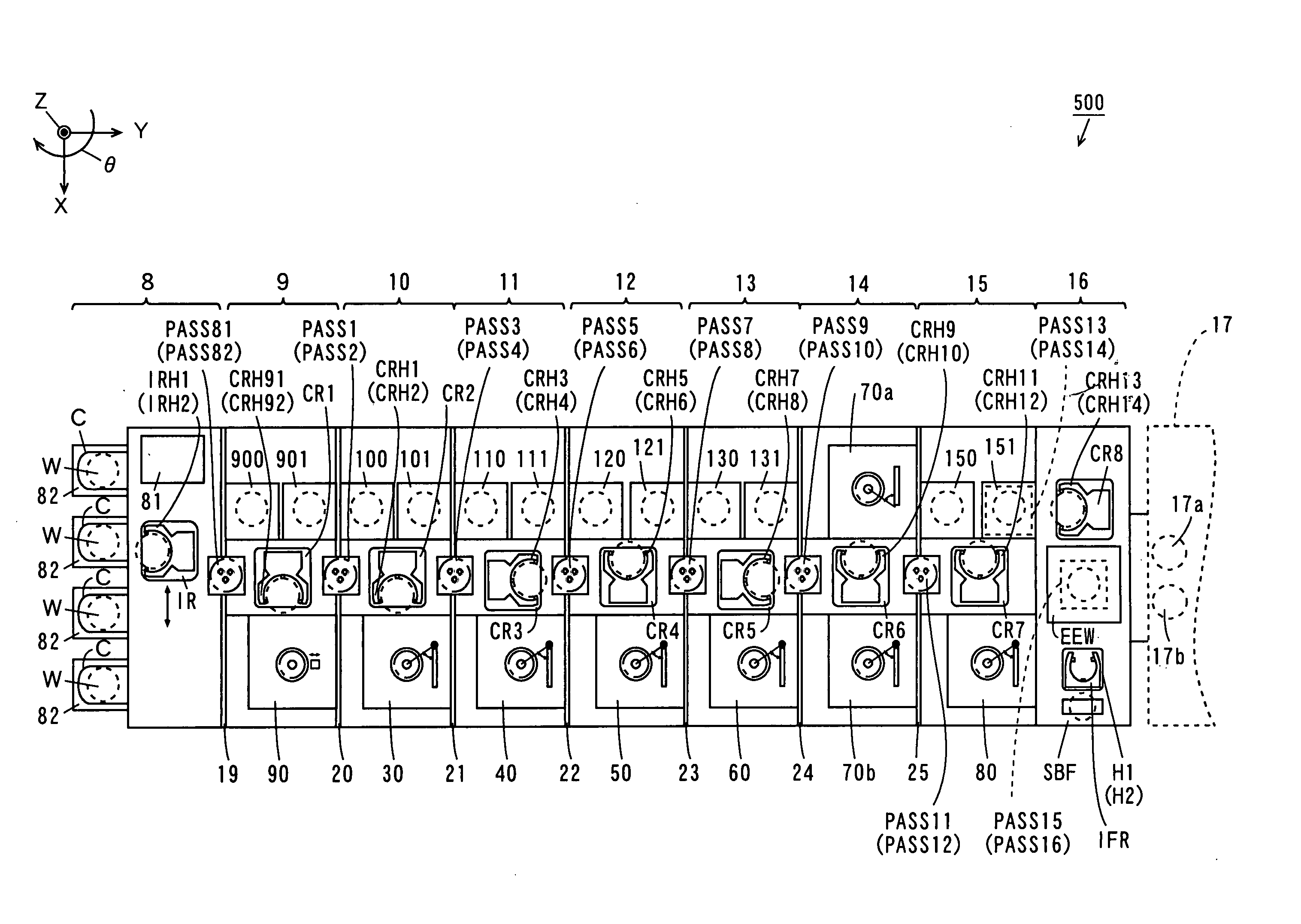
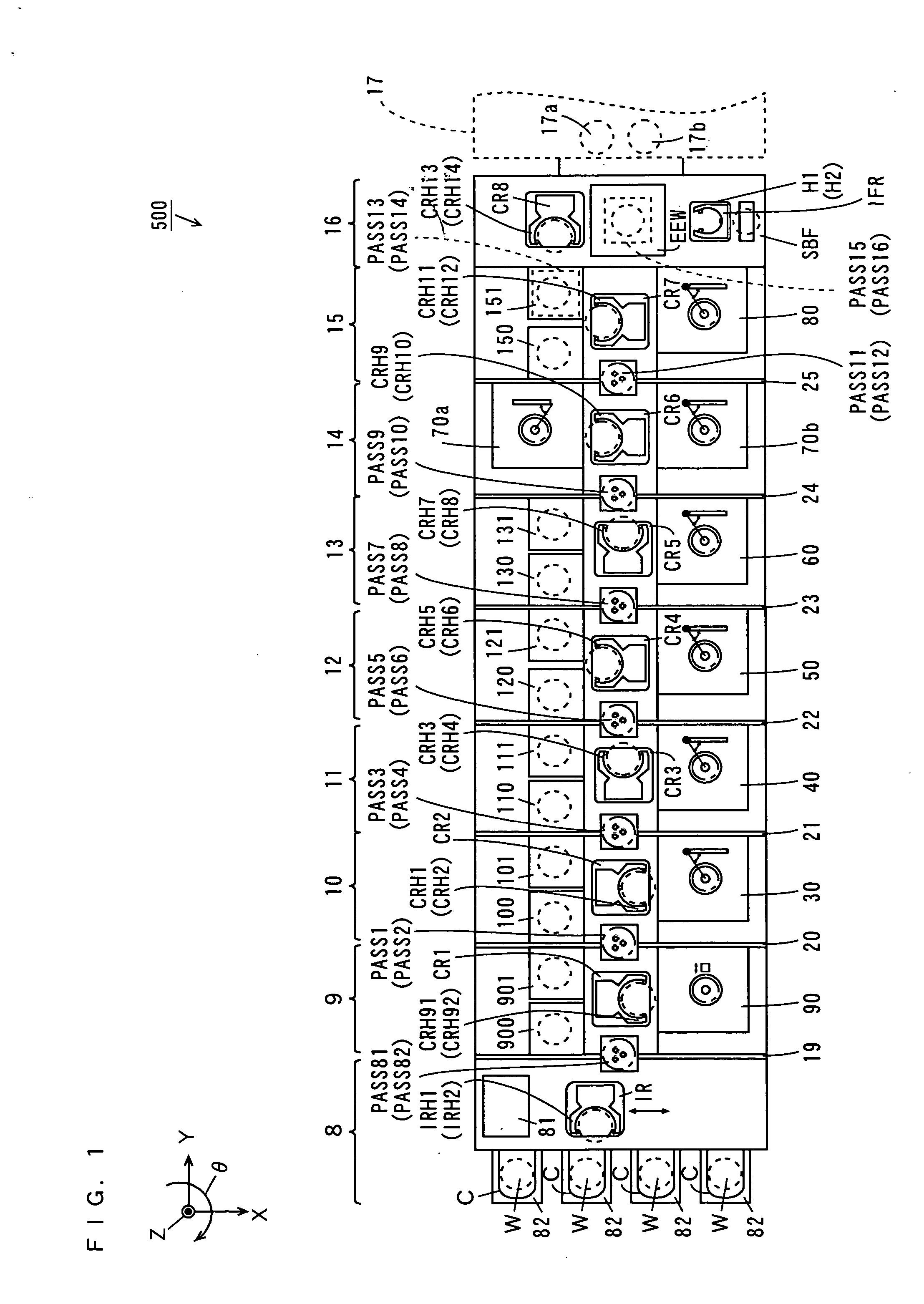
[0145]FIG. 1 is a schematic plan view of a substrate processing apparatus according to a first embodiment of the invention.

[0146] As shown in FIG. 1, a substrate processing apparatus 500 includes an indexer block 8, an edge-cleaning processing block 9, an anti-reflection film processing block 10, a resist film processing block 11, a development processing block 12, a resist cover film processing block 13, a resist cover film removal block 14, an cleaning / drying processing block 15 and an interface block 16. In the substrate processing apparatus 500, these blocks are provided in the above order.

[0147] An exposure device 17 is arranged adjacent to the interface block 16 of the substrate processing apparatus 500. The exposure device 17 applies the exposure processin...

Example

B. The Second Embodiment

[0413] The substrate processing apparatus according to the second embodiment is different from the substrate processing apparatus 500 according to the first embodiment as described below.

[0414] (1) Configuration of the Substrate Processing Apparatus

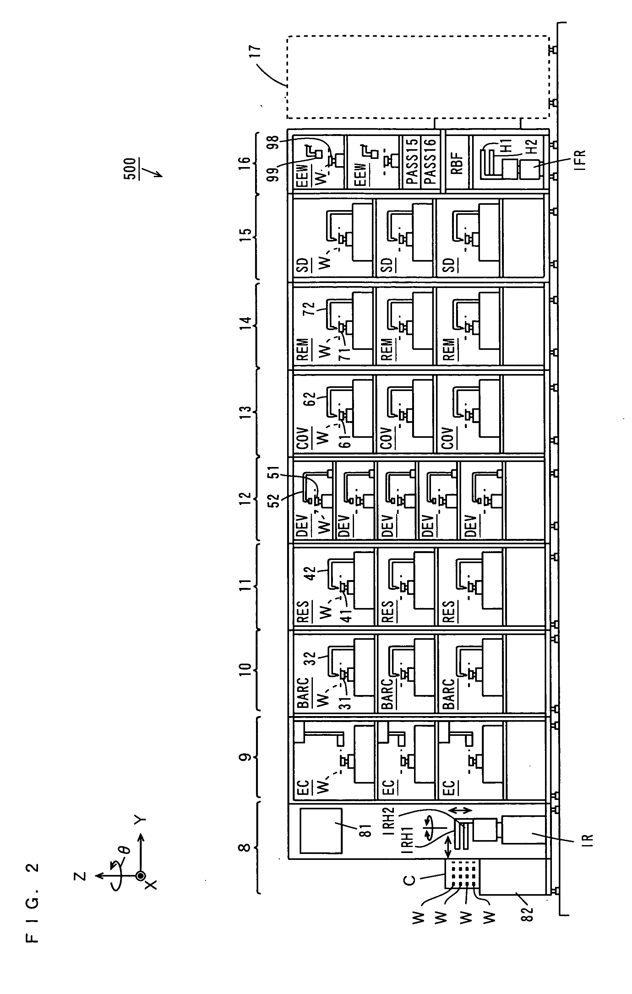
[0415]FIG. 21 is a schematic plan view of a substrate processing apparatus according to the second embodiment.

[0416] As shown in FIG. 21, the edge-cleaning processing block 9 of the substrate processing apparatus 500 according to the first embodiment is not provided in the substrate processing apparatus 500 according to this embodiment. Therefore, the indexer block 8 is provided adjacent to the anti-reflection film processing block 10.

[0417] A partition wall 20 is thus arranged between the indexer block 8 and the anti-reflection film processing block 10 for shielding an atmosphere. The partition wall 20 has substrate platforms PASS1, PASS2 provided closely one above the other for receiving and transferring the...


PUM


Abstract

A substrate processing apparatus comprises an indexer block, an edge-cleaning processing block, an anti-reflection film processing block, a resist film processing block, a development processing block, a resist cover film processing block, a resist cover film removal block, a cleaning/drying processing block and an interface block. An exposure device is arranged adjacent to the interface block of the substrate processing apparatus. In the exposure device, exposure processing is applied to a substrate by a liquid immersion method. In the edge-cleaning processing group in the edge-cleaning processing block, an edge of the substrate before exposure processing is cleaned.

Description

BACKGROUND OF THE INVENTION [0001] 1. Field of the Invention [0002] The present invention relates to a substrate processing apparatus for applying processing to substrates. [0003] 2. Description of the Background Art [0004] A substrate processing apparatus is used to apply a variety of processing to substrates such as semiconductor substrates, substrates for use in liquid crystal displays, plasma displays, optical disks, magnetic disks, magneto-optical disks, photomasks, and other substrates. [0005] Such a substrate processing apparatus typically applies a plurality of successive processing to a single substrate. The substrate processing apparatus as described in JP 2003-324139 A includes an indexer block, an anti-reflection film processing block, a resist film processing block, a development processing block, and an interface block. An exposure device is arranged adjacent to the interface block as an external device separate from the substrate processing apparatus. [0006] In the ab...

Claims


Application Information

Patent Timeline
IPC IPC(8): G03D5/00G03F7/30G03F7/38H01L21/027H01L21/304
CPCG03F7/00G03F7/162G03F7/168G03F7/2041H01L21/02087H01L21/67742H01L21/67051H01L21/6708H01L21/67173H01L21/67178H01L21/67225H01L21/67034Y10S134/902H01L21/0274H01L21/3046H01L21/67017
Inventor SHIGEMORI, KAZUHITOKANEYAMA, KOJIHARUMOTO, AKIKOMIYAGI, TADASHIKANAOKA, MASASHIYASUDA, SHUICHI
Owner SCREEN SEMICON SOLUTIONS CO LTD
Why Eureka
Try Eureka