Etching of silicon nitride with improved nitride-to-oxide selectivity utilizing halogen bromide/chlorine plasma

Pending Publication Date: 2006-12-28
UNITED MICROELECTRONICS CORP
View PDF2 Cites 6 Cited by
  • Summary
  • Abstract
  • Description
  • Claims
  • Application Information

AI Technical Summary

Benefits of technology

[0008] It is the primary object of the present invention to provide a met

Problems solved by technology

The above-described prior art method has several disadvantages, one o

Method used


Image

  • Etching of silicon nitride with improved nitride-to-oxide selectivity utilizing halogen bromide/chlorine plasma
  • Etching of silicon nitride with improved nitride-to-oxide selectivity utilizing halogen bromide/chlorine plasma
  • Etching of silicon nitride with improved nitride-to-oxide selectivity utilizing halogen bromide/chlorine plasma

Examples


Example

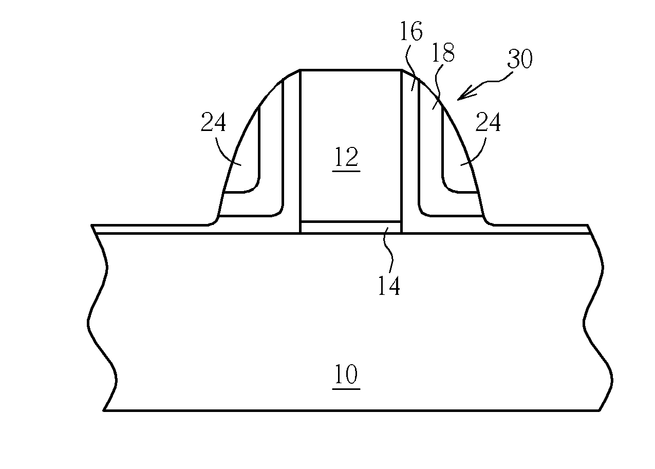
[0016] The present invention pertains to a semiconductor etching process utilizing hydrogen bromide and chlorine (HBr / Cl2) as plasma source gases for improving nitride-to-oxide selectivity. Exemplary embodiments from different aspects of this invention are proposed with reference to the accompanying figures. These exemplary embodiments can be performed in a Lam 2300 series etcher tool available from Lam Research Corp. or in other similar etcher tools that are capable of providing source power (i.e., top power) and bias power (i.e., bottom power). Hereinafter, the nitride-to-oxide selectivity is defined as the ratio of etching rate of silicon nitride to the etching rate of silicon oxide.

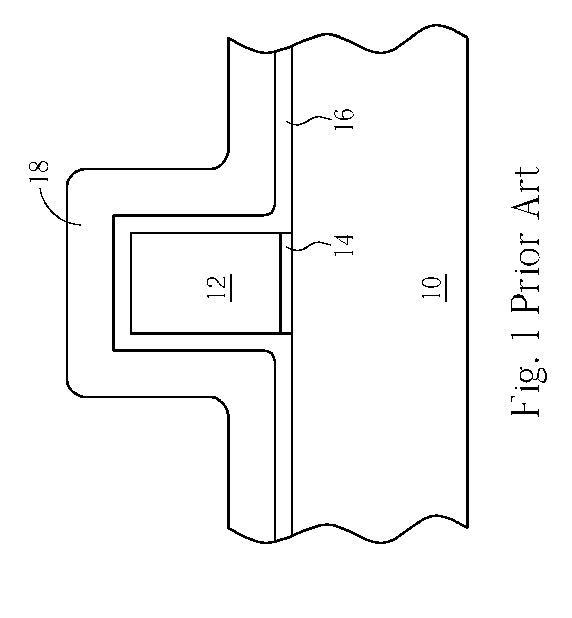
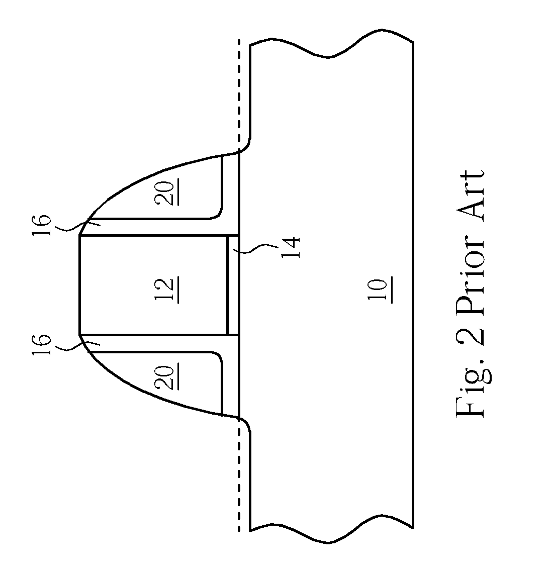
[0017] Please refer to FIG. 3 and FIG. 4. FIG. 3 and FIG. 4 are schematic, cross-sectional diagrams illustrating the etching of silicon nitride spacers utilizing HBr / Cl2 plasma in accordance with the first preferred embodiment of this invention. As shown in FIG. 3, a gate 12 having a gate channel len...


PUM


Abstract

A method of manufacturing a semiconductor device is disclosed. A gate is formed on a semiconductor substrate. A gate oxide is formed between the gate and the semiconductor substrate. A silicon oxide liner layer is deposited on the gate and on the semiconductor substrate. A silicon nitride layer is then deposited on the silicon oxide liner layer. The silicon nitride layer is anisotropically etched by employing plasma created by using plasma source gas containing hydrogen bromide and chlorine thereby forming spacer on sidewalls of the gate. The hydrogen bromide plasma is produced at a temperature of about 50-150° C., a pressure of 5-200 mTorr, a source power of no less than 800 Watts, and a bias power of about 100-200 Watts.

Description

BACKGROUND OF THE INVENTION [0001] 1. Field of the Invention [0002] The present invention relates generally to a method of making a semiconductor device and, more particularly, to a method of etching silicon nitride with improved nitride-to-oxide selectivity utilizing hydrogen bromide / chlorine (HBr / Cl2) plasma. [0003] 2. Description of the Prior Art [0004] Dimensional control in etching small features, necessary for advanced micromachining, is an important topic in silicon technology. To etch these structures, dry plasma-assisted etching is increasingly used. In the fabrication of semiconductor devices, it is often desirable to dry etch silicon nitride with high selectivity relative to silicon oxide. [0005]FIG. 1 and FIG. 2 are schematic diagrams showing the method of making silicon nitride spacer on gate sidewalls according to the prior art. As shown in FIG. 1, a gate 12 is formed on the main surface of the semiconductor substrate 10. Between the gate 12 and the semiconductor subst...

Claims


Application Information

Patent Timeline
IPC IPC(8): H01L21/302
CPCH01L21/31116H01L21/31144H01L29/6656H01L21/76811H01L21/76802
Inventor TSAI, CHANG-HU
Owner UNITED MICROELECTRONICS CORP
Why Eureka
Try Eureka