Stacked photovoltaic device

a photovoltaic device and stacked technology, applied in the direction of semiconductor devices, electrical equipment, basic electric elements, etc., can solve the problems that the initial characteristics of the second photovoltaic unit are not provided a significant influence on the device at large, and achieve the effect of improving the total generated energy in the long-term service, increasing oxygen content, and increasing reaction pressur

Inactive Publication Date: 2007-01-04
SANYO ELECTRIC CO LTD
View PDF3 Cites 13 Cited by
  • Summary
  • Abstract
  • Description
  • Claims
  • Application Information

AI Technical Summary

Benefits of technology

[0010] In the present invention, α2 is rendered larger than α1, as described above. This causes slight degradation of initial characteristics but is effective in retarding photodegradation in the long-term service. Thus, total generated energy in the long-term service is improved, relative to conventional devices.
[0011] In the present invention, α2 of the microcrystalline silicon layer in the second photovoltaic unit is designed to exceed α1 of the amorphous silicon layer in the first photovoltaic unit. This design can be realized by increasing an oxygen content of the microcrystalline silicon layer in the second photovoltaic unit. The oxygen content can be increased, for example, by increasing a reaction pressure when a thin film is formed or decreasing a hydrogen concentration when a reaction gas is diluted with hydrogen. Alternatively, oxygen can be introduced in the microcrystalline silicon layer by adding an oxygen-containing gas, such as CO2, to a reaction gas. Such incorporation of oxygen into the microcrystalline silicon layer increases its Si—O bond content and renders α2 greater than α1.

Problems solved by technology

Since an overall short-circuit current of the stacked photovoltaic device is governed by the current value of the photovoltaic unit having a smaller short-circuit current, degradation of the initial characteristics of the second photovoltaic unit does not provide a significant influence on the device at large.

Method used


Image

  • Stacked photovoltaic device
  • Stacked photovoltaic device
  • Stacked photovoltaic device

Examples


example

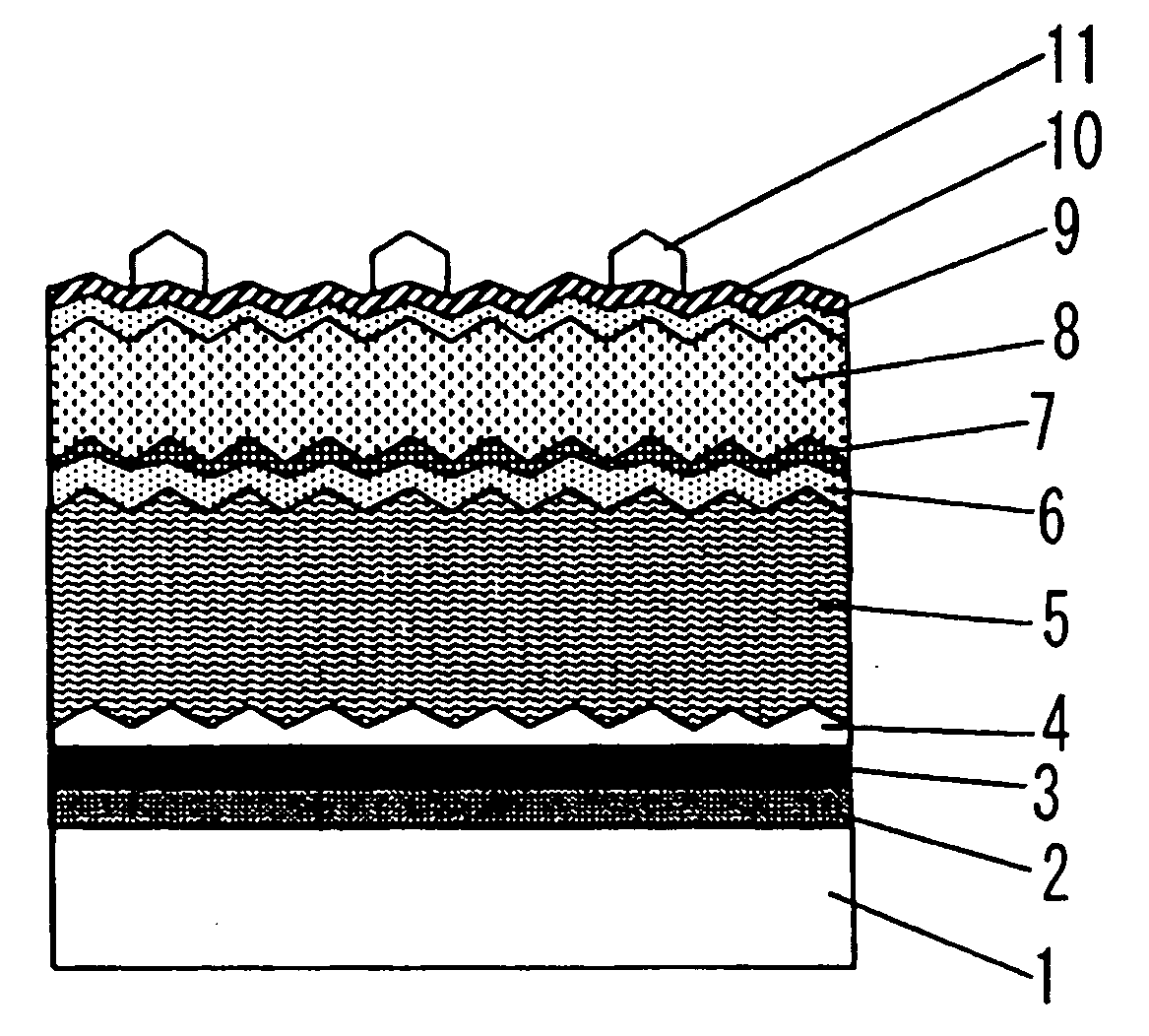
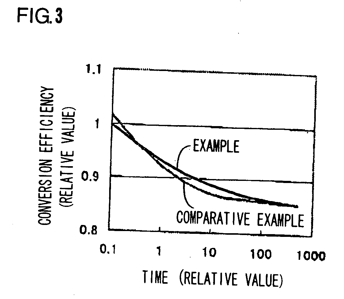
[0034]FIG. 1 is a sectional view showing a stacked photovoltaic device in accordance with an embodiment of the present invention. The stacked photovoltaic device (tandem type photovoltaic device) shown in FIG. 1 includes a first photovoltaic unit using an amorphous silicon layer as a photoelectric conversion layer and a second photovoltaic unit using a microcrystalline silicon layer as a photoelectric conversion layer, arranged in the sequence closer to a light incidence plane.

[0035] As shown in FIG. 1, a substrate 1 carries thereon a polyimide layer 2 on which a back electrode 3 is disposed. An n-type microcrystalline silicon (μc-Si:H) layer 4 (20 nm thick), an intrinsic (i-type) microcrystalline silicon (μc-Si:H) layer 5 (2 μm thick) serving as a photoelectric conversion layer and a p-type microcrystalline silicon (μc-Si:H) layer 6 (20 nm thick) are sequentially formed on the back electrode 3. These n-type, intrinsic and p-type microcrystalline silicon layers 4, 5 and 6 constitut...


PUM


Abstract

A stacked photovoltaic device which includes a first photovoltaic unit having an amorphous silicon layer 8 as a photoelectric conversion layer, and a second photovoltaic unit having a microcrystalline silicon layer 5 as a photo-electric conversion layer and succeeding backwardly from the first photovoltaic unit closer to a light incidence plane. The microcrystalline silicon layer 5 serving as the photoelectric conversion layer in the second photovoltaic unit has a ratio α2(=I(Si—O)/I(Si—H)) greater than a ratio α1(=I(Si—O)/I(Si—H)) of the amorphous silicon layer 8 serving as the photoelectric conversion layer in the first photovoltaic unit, where I(Si—O) is a peak area for the Si—O stretching mode of each silicon layer and I(Si—H) is a peak area for the Si—H stretching mode of each silicon layer when the amorphous and microcrystalline silicon layers 8 and 5 are measured by infrared absorption spectroscopy. Also, a short-circuit current Isc2 of the second photovoltaic unit is greater than a short-circuit current Isc1 of the first photovoltaic unit.

Description

BACKGROUND OF THE INVENTION [0001] 1. Field of the Invention [0002] The present invention relates to a stacked photovoltaic device which includes a photovoltaic unit having an amorphous silicon layer serving as a photoelectric conversion layer, and a photovoltaic unit having a microcrystalline silicon layer serving as a photoelectric conversion layer and succeeding backwardly from the former photovoltaic unit closer to a light incidence plane. [0003] 2. Description of the Related Art [0004] A stacked photovoltaic device consisting of a multilayer of photovoltaic units is known to improve a photoelectric conversion efficiency. In order to improve a photoelectric conversion efficiency, such a stacked photovoltaic device is built by stacking photovoltaic units having different band gaps which absorb lights in respective regions of the solar spectrum. [0005] This type of stacked photovoltaic unit is proposed such as in Japanese Patent Laying-Open No. Hei 11-243218. It uses amorphous sil...

Claims


Application Information

Patent Timeline
Patent Type & Authority Applications(United States)
IPC IPC(8): H01L31/00H01L31/06H01L31/076H01L31/077
CPCH01L31/03685H01L31/0725Y02E10/545Y02E10/548H01L31/076Y02E10/547
Inventor SHIMA, MASAKI
Owner SANYO ELECTRIC CO LTD
Why Eureka
Try Eureka