(Al, Ga, In)N and ZnO direct wafer bonded structure for optoelectronic applications, and its fabrication method

Inactive Publication Date: 2007-01-04
JAPAN SCI & TECH CORP
View PDF31 Cites 69 Cited by
  • Summary
  • Abstract
  • Description
  • Claims
  • Application Information

AI Technical Summary

Benefits of technology

[0026] The method may further comprise enhancing electrical conductivity of a wafer bonded interface prior to direct wafer bonding. The transparent conductor layers' surface may be plasma treated prior to the wafer bonding pro

Problems solved by technology

Also, surface feature shaping for improving light extraction efficiency is difficult because of the hardness of GaN material and the instability of p-type GaN conductivity.
However, this method requires using ZnO

Method used


Image

  • (Al, Ga, In)N and ZnO direct wafer bonded structure for optoelectronic applications, and its fabrication method
  • (Al, Ga, In)N and ZnO direct wafer bonded structure for optoelectronic applications, and its fabrication method
  • (Al, Ga, In)N and ZnO direct wafer bonded structure for optoelectronic applications, and its fabrication method

Examples


Embodiment Construction

[0049] In the following description of the preferred embodiment, reference is made to the accompanying drawings which form a part hereof, and in which is shown by way of illustration a specific embodiment in which the invention may be practiced. It is to be understood that other embodiments may be utilized and structural changes may be made without departing from the scope of the present invention.

[0050] Overview

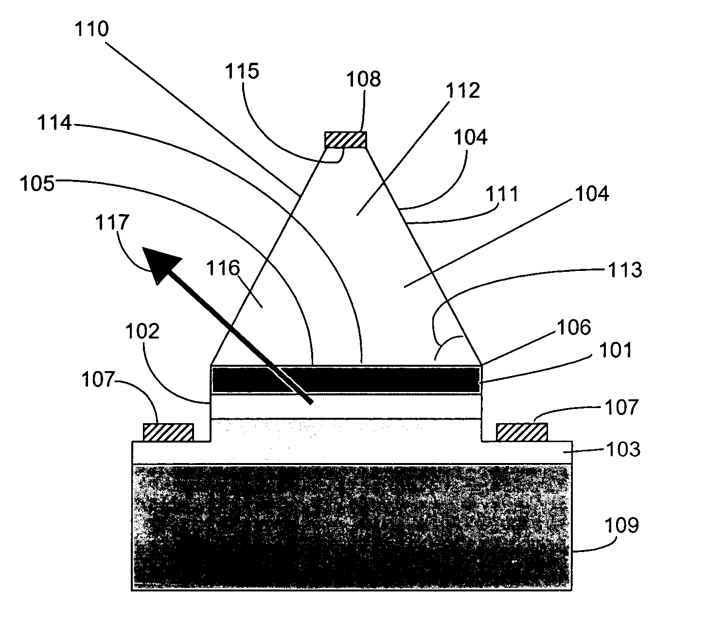
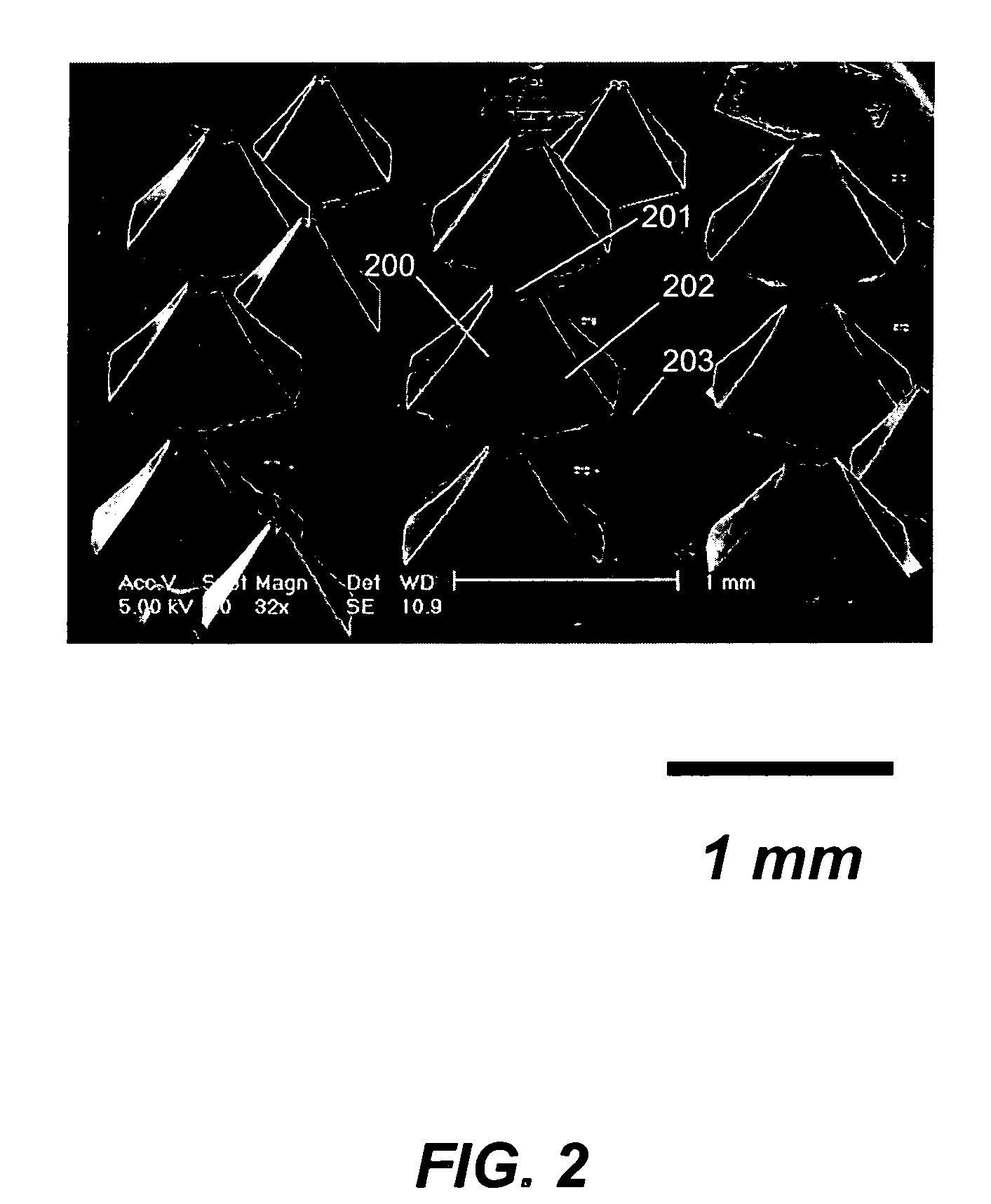
[0051] The purpose of the present invention is to provide a means of increasing the light extraction efficiency from an LED by the direct wafer bonding of (Al, Ga, In)N and ZnO wafers followed by ZnO shaping.

[0052] Producing highly transparent and conductive electrodes, especially surface feature shaped electrode fabrication on p-type GaN, is difficult. Conventionally, a thin metal combination of Ni and Au is used for the p-electrode, which has a transmittance of only around 60% for optical wavelengths of less than 470 nm.

[0053] On the other hand, a ZnO wafer is highly t...


PUM

PropertyMeasurementUnit
Temperatureaaaaaaaaaa
Timeaaaaaaaaaa
Temperatureaaaaaaaaaa

Abstract

An (Al, Ga, In)N and ZnO direct wafer bonded light emitting diode (LED), wherein light passes through electrically conductive ZnO. Flat and clean surfaces are prepared for both the (Al, Ga, In)N and ZnO wafers. A wafer bonding process is then performed between the (Al, Ga, In)N and ZnO wafers, wherein the (Al, Ga, In)N and ZnO wafers are joined together and then wafer bonded in a nitrogen ambient under uniaxial pressure at a set temperature for a set duration. After the wafer bonding process, ZnO is shaped for increasing light extraction from inside of LED.

Description

CROSS-REFERENCE TO RELATED APPLICATIONS [0001] This application claims the benefit under 35 U.S.C. Section 119(e) of the following co-pending and commonly-assigned U.S. patent applications: [0002] U.S. Provisional Application Ser. No. 60 / 691,710, filed on Jun. 17, 2005, by Akihiko Murai, Christina Ye Chen, Lee S. McCarthy, Steven P. DenBaars, Shuji Nakamura, and Umesh K. Mishra, entitled “(Al,Ga,In)N AND ZnO DIRECT WAFER BONDING STRUCTURE FOR OPTOELECTRONIC APPLICATIONS AND ITS FABRICATION METHOD,” attorneys' docket number 30794.134-US-P1 (2005-536-1); [0003] U.S. Provisional Application Ser. No. 60 / 732,319, filed on Nov. 1, 2005, by Akihiko Murai, Christina Ye Chen, Daniel B. Thompson, Lee McCarthy, Steven P. DenBaars, Shuji Nakamura, and Umesh K. Mishra, entitled “(Al, Ga, In)N AND ZnO DIRECT WAFER BONDED STRUCTURE FOR OPTOELECTRONIC APPLICATIONS, AND ITS FABRICATION METHOD,” attorneys' docket number 30794.134-US-P2 (2005-536-2); and [0004] U.S. Provisional Application Ser. No. 60...

Claims


Application Information

Patent Timeline
IPC IPC(8): H01L33/00H01L21/00H01L33/20H01L33/22H01L33/32
CPCH01L33/0079H01L33/20H01L33/22H01L33/32H01S5/32341H01S5/0421H01S5/18347H01S5/18369H01S5/1838H01S5/0215H01L33/0093
Inventor MURAI, AKIHIKOCHEN, CHRISTINA YETHOMPSON, DANIEL B.MCCARTHY, LEE S.DENBAARS, STEVEN P.NAKAMURA, SHOJIMISHRA, UMESH K.
Owner JAPAN SCI & TECH CORP
Why Eureka
Try Eureka