This helps you quickly interpret patents by identifying the three key elements:
Problems solved by technology
Method used
Benefits of technology
Benefits of technology
[0010] Accordingly, it is an object of the present invention to provide a bonding apparatus and method capable of efficiently performing surface treatments and bonding processing on bonding subjects on which bonding is executed.
[0011] It is another object of the present invention to provide a bonding apparatus and method that makes it possible to effect surface treatments on bonding subjects using microplasma.
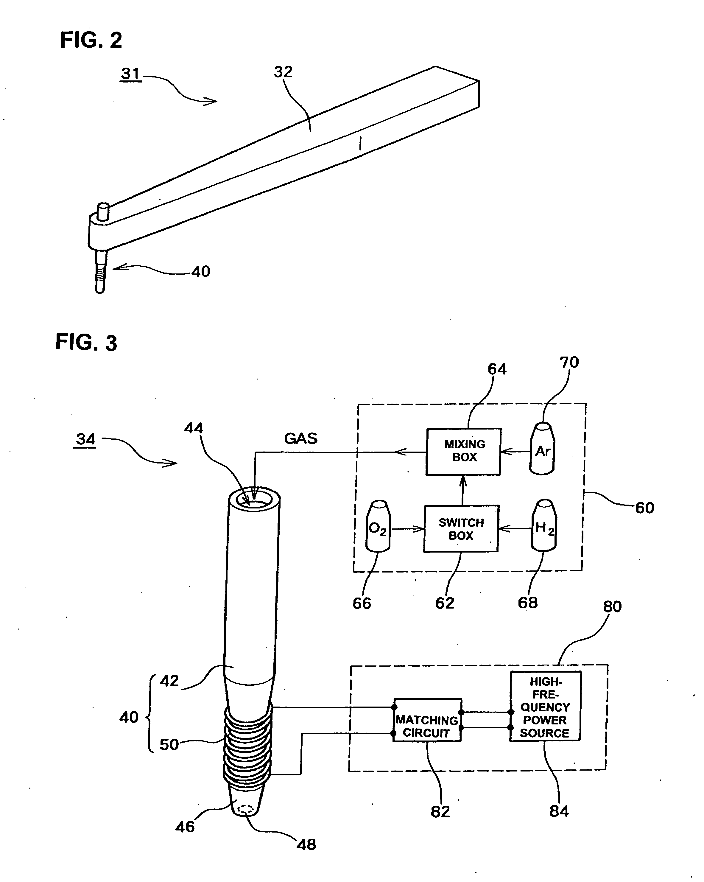
[0049] With the structures described above, in addition to a bonding processor, the bonding apparatus and method of the present invention is provided with an inductivety coupled microplasma generator that includes a plasma capillary having a high-frequency coil wound on the tip end portion thereof and performs surface treatment by ejecting gas being a plasma in the interior of the plasma capillary by the supply of electric power to the high-frequency coil, onto a bonding subject from the opening in the tip end portion of the plasma capillary. Accordingly, both a bonding processing function and a function for performing surface treatments, with little heat damage, by irradiating the bonding subject in a small area with the microplasma, are involved, and surface treatment and bonding processing are efficiently performed on the bonding subject.
[0053] Furthermore, the bonding processing and surface treatments for the same bonding subject are interconnectedly performed in the present invention. Accordingly, surface treatment and bonding processing are done simultaneously, in parallel, or sequentially, on one chip, for example, and thus it is possible to perform bonding processing immediately after surface treatment.
[0054] Furthermore, since the bonding arm and the plasma arm are moved as one unit in the present invention, the movement mechanism can be simple in structure.
[0055] As seen from the above according to the bonding apparatus and method of the present invention, it is possible to perform surface treatment and bonding processing on bonding subjects efficiently. It is further possible in the present invention to perform surface treatments on bonding subjects with microplasma.
Problems solved by technology
More specifically, when the surface of either the metal layer of a bonding pad or the metal layer of a bonding lead is contaminated, or foreign matter is present thereon, then it is not possible to obtain a good electrical junction between such surface and the fine metal wire, and the strength of the mechanical junction is also weak.
This method is a capacitively coupled plasma generating method, and involves electrical discharges; accordingly, there are effects damage to electronic devices.
As seen from the above, in the bonding apparatuses of the conventional art, it is very difficult to perform surface treatment that is efficient, with the relationship with bonding processing.
Method used
Image
Click on the blue label to locate the original text in one second.
Reading with bidirectional positioning of images and text.
Examples
embodiment 1
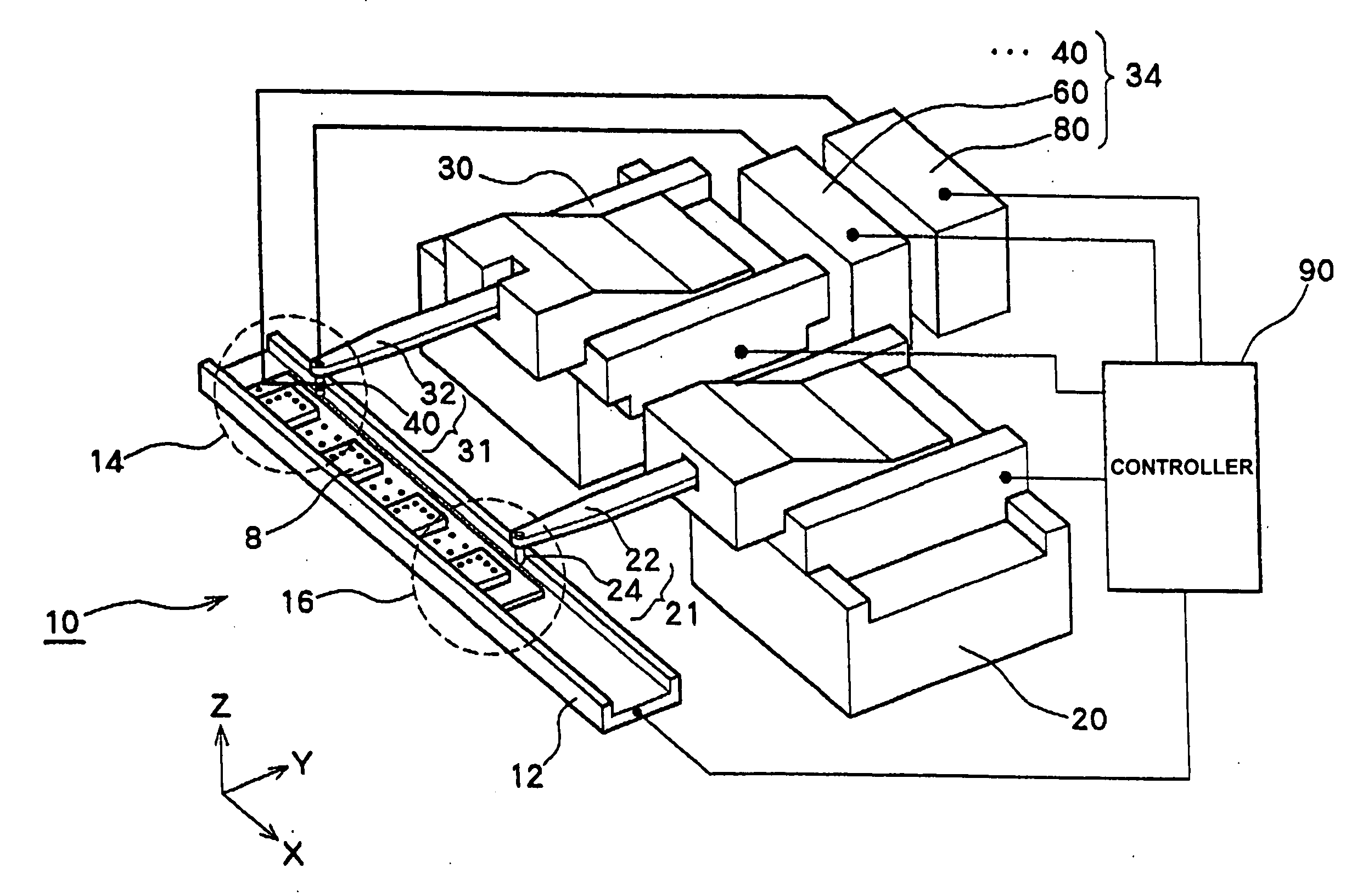
[0074]FIG. 1 shows a wire bonding apparatus 10 capable of performing surface treatments and bonding processing. Chips mounted on a substrate are also shown as bonding subjects 8. The wire bonding apparatus 10 has functions for performing a surface treatment by the action of the plasma-state gas, prior to the bonding processing, on a narrow area for performing bonding, specifically on a chip bonding pad and board bonding leads, for a bonding subject 8, and then performing bonding processing.
[0075] The wire bonding apparatus 10 is comprised of a transporter mechanism 12 for holding the bonding subject 8 and transporting it to a prescribed position, a bonding arm 21 having a bonding capillary 24 attached to the tip end of a bonding arm main body 22, a bonding XYZ drive mechanism 20 for movement-driving the bonding arm 21, a plasma arm 31 having a plasma capillary 40 attached to the tip end of a plasma arm main body 32, a surface treatment XYZ drive mechanism 30 for movement-driving th...
embodiment 2
[0105] The microplasma generator 34 shown in FIG. 3 can be applied to a bump bonding apparatus. A bump bonding apparatus is an apparatus for forming metal bumps in flip chip technology. More specifically, such an apparatus uses the principle of wire bonding to a bonding pad on a chip to bond metal wires and make those metal bumps. Thus it might be characterized as equivalent to an ordinary wire bonding process from which the second bonding is eliminated. Accordingly, such an apparatus corresponds to the wire bonding apparatus 10 shown in FIG. 1, in which the bonding subject 8 transported by the transporter mechanism 12 has been made a completed wafer on which completed LSIs are arrayed.
[0106] When the bonding subject 8 is a completed wafer, in the surface treatment stage 14, bonding pads 5 are surface-treated, respectively, for a plurality of completed LSIs. Then, when surface treatment on all of the bonding pads has been completed for one completed wafer, the bonding subject 8 is ...
embodiment 3
[0111] The microplasma generator 34 shown in FIG. 3 can be applied to a flip chip bonding apparatus. A flip chip bonding apparatus is an apparatus for placing a chip on which a bump is formed as shown in FIGS. 7(a) through 7(c) face down on a circuit board. Accordingly, in such cases, the bump 3 on the chip 6 and the bonding lead 4 connected. Furthermore, the chip is inverted in order to place it face down, and the bonding tool for effecting facedown bonding is not a bonding capillary but a collet for holding the chip placed face down. Thus the specific configuration of a flip chip bonding apparatus differs considerably from that of a wire bonding apparatus.
[0112] There are two stages in applying the microplasma generator 34 in a flip chip bonding apparatus, namely when surface-treating the chip bump 3, before inverting the chip and holding it with the collet, and when surface-treating the bonding lead 4 before effecting facedown bonding with the collet
[0113] FIGS. 8(a) through 8(...
PUM
Property
Measurement
Unit
Frequency
aaaaa
aaaaa
Abstract
A wire bonding apparatus 10 including an XYZ drive mechanism 20 for moving a bonding arm 21 that has a bonding capillary 24 at its tip end, an XYZ drive mechanism 30 for driving a plasma arm 31 that has a plasma capillary 40 having a high-frequency coil wound at its tip end portion end, a gas supply unit 60 for supplying gas to the plasma capillary, and a high-frequency power supply unit 80 for supplying high-frequency electric power to the high-frequency coil. With a supply of high-frequency electric power to the high-frequency coil, gas is being a plasma inside the plasma capillary and is ejected from its tip end against a bonding subject 8, thus performing surface treatment on the bonding subject; and using the bonding capillary, bonding is performed interconnectedly with this surface treatment.
Description
BACKGROUND OF THE INVENTION [0001] The present invention relates to a bonding apparatus and method and more particularly to a bonding apparatus and method for executing a bonding process after performing a surface treatment on a bonding subject on which bonding is executed. [0002] Bonding apparatuses are generally for making connections between chipelectrode units and circuit board lead terminals with fine metal wires. Chipelectrode units connected by fine metal wires are sometimes called bonding pads, and circuit board lead terminals are sometimes called bonding leads. When fine metal wires are connected to these elements using ultrasonic connection technology or thermo-compression bonding or the like, it is important to know surface conditions thereof. More specifically, when the surface of either the metal layer of a bonding pad or the metal layer of a bonding lead is contaminated, or foreign matter is present thereon, then it is not possible to obtain a good electrical junctio...
Claims
Application Information
Patent Timeline
Application Date:The date an application was filed.
Publication Date:The date a patent or application was officially published.
First Publication Date:The earliest publication date of a patent with the same application number.
Issue Date:Publication date of the patent grant document.
PCT Entry Date:The Entry date of PCT National Phase.
Estimated Expiry Date:The statutory expiry date of a patent right according to the Patent Law, and it is the longest term of protection that the patent right can achieve without the termination of the patent right due to other reasons(Term extension factor has been taken into account ).
Invalid Date:Actual expiry date is based on effective date or publication date of legal transaction data of invalid patent.

