Apparatus and method for canceling DC output offset

a technology of output power and offset, applied in the field of semiconductor circuits, can solve the problems of large current consumption, large area covered by capacitors and digital circuit blocks, and inability to use such capacitors or digital blocks, and achieve the effect of low power consumption

Inactive Publication Date: 2007-01-04
SAMSUNG ELECTRONICS CO LTD
View PDF5 Cites 7 Cited by
  • Summary
  • Abstract
  • Description
  • Claims
  • Application Information

AI Technical Summary

Benefits of technology

[0007] The present invention provides an apparatus and method for substantially canceling a direct current (DC) offset occurring between input signals of a mixer while realizing compactness and low power consumption.

Problems solved by technology

In particular, since carrier leakage is very sensitive to the DC offset, it greatly degrades adjacent channel power rejection (ACPR) and a maximum output power dynamic range.
However, when a capacitor with large capacitance is provided or digital circuit blocks such as an analog-to-digital converter and a digital-to-analog converter are implemented in the DCT to reduce the DC offset, the capacitor and the digital circuit blocks cover a large area and have a large current consumption.
Accordingly, use of such capacitors or digital blocks is not appropriate to a trend toward compactness and low power consumption in the communications market.

Method used


Image

  • Apparatus and method for canceling DC output offset
  • Apparatus and method for canceling DC output offset
  • Apparatus and method for canceling DC output offset

Examples


Embodiment Construction

[0022] The present invention will be described with reference to the attached drawings, wherein like reference numerals refer to like elements throughout.

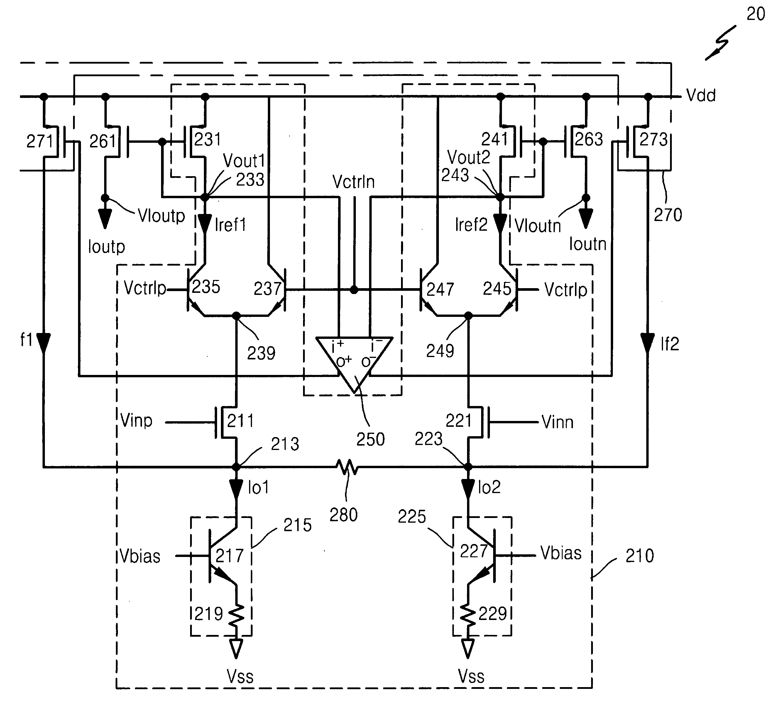
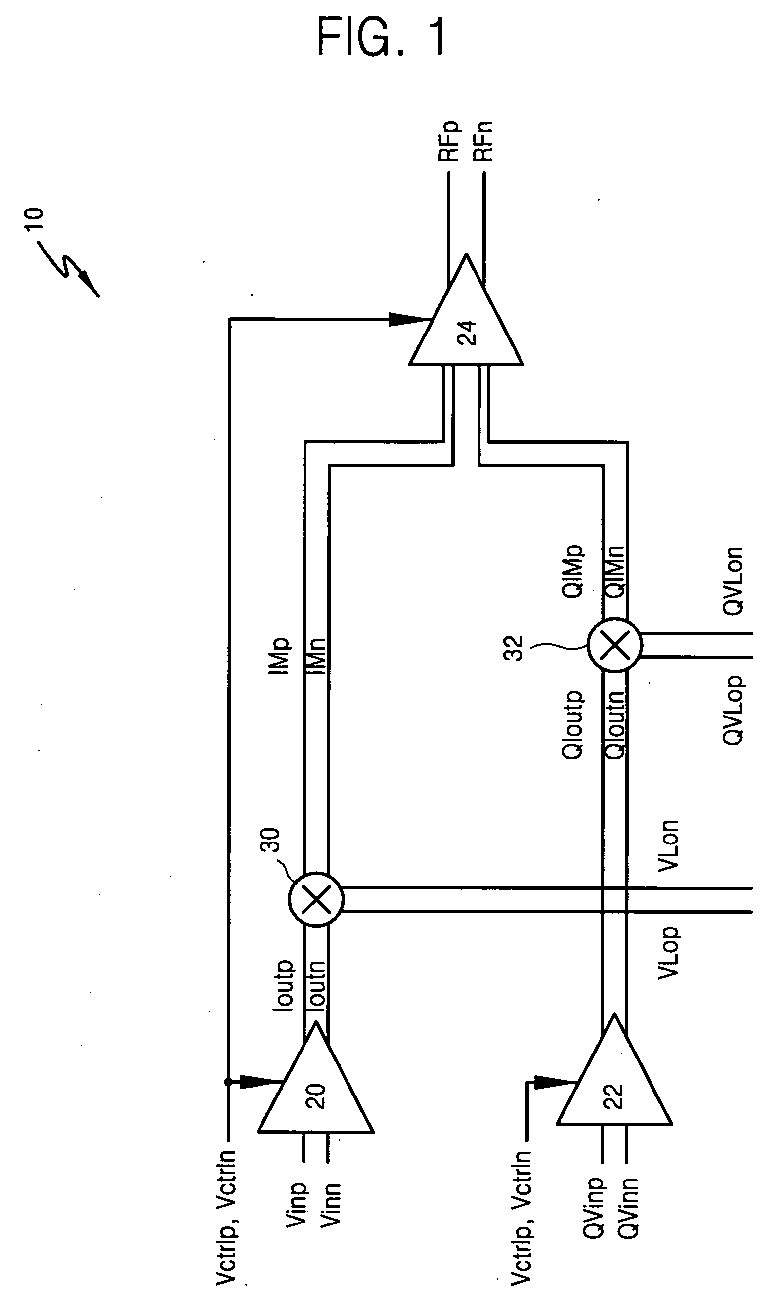
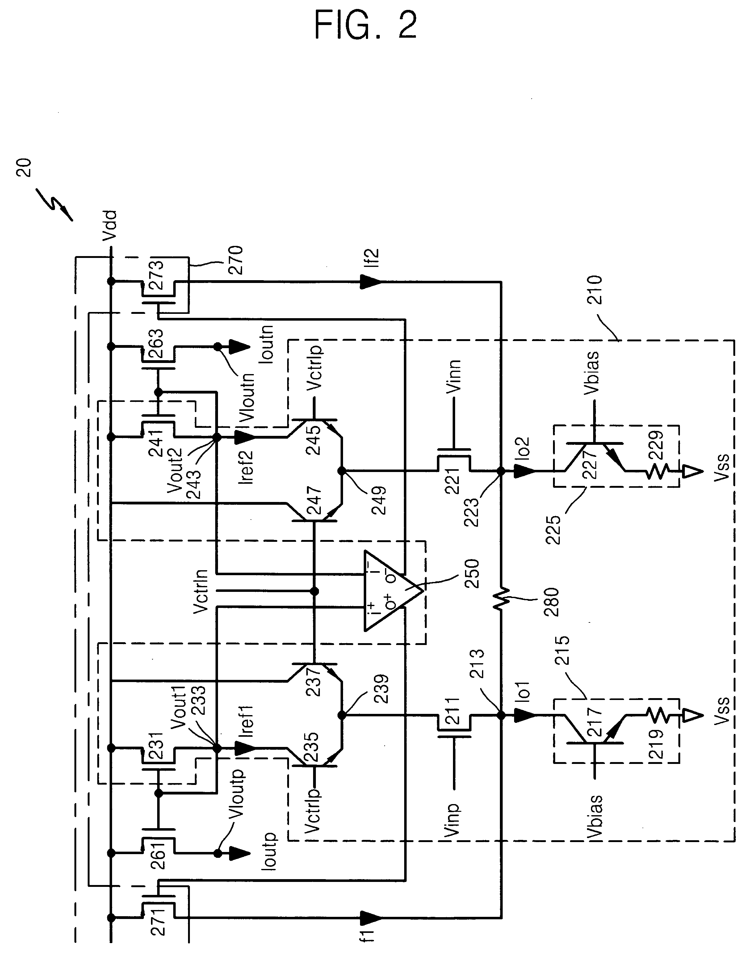
[0023]FIG. 1 is a block diagram of a transmitter including transconductors according to an embodiment of the present invention. The transmitter 10 may be used for wideband code-division multiple access (WCDMA). FIG. 2 is a circuit diagram of a transconductor of FIG. 1 according to an embodiment of the present invention.

[0024] Referring to FIGS. 1 and 2, the transmitter 10 includes a plurality of transconductors, for example first and second transconductors 20 and 22, a variable gain amplifier 24, and a plurality of mixers, for example first and second mixers 30 and 32. Each of the first and second transconductors 20 and 22 receives signals output from a modem (not shown) or a baseband low-pass filter (not shown).

[0025] The first transconductor 20 is controlled by first and second control signals Vctrlp and Vctrln and outputs var...


PUM


Abstract

A transconductor for substantially canceling or reducing a direct current (DC) output offset and a method thereof are provided. The transconductor includes a differential amplifier, a sensing circuit, and a feedback current generation circuit. The differential amplifier outputs output signals having a DC output offset therebetween due to a difference between input signals or a mismatch between input terminals. The sensing circuit senses the DC output offset and outputs a sensing signal. The feedback current generation circuit provides a feedback current for adjusting a level of the output signals to the input stage of the differential amplifier in response to the sensing signal. Accordingly, the transconductor substantially cancels or reduces the DC output offset between the output signals in response to the feedback current.

Description

CROSS-REFERENCE TO RELATED PATENT APPLICATIONS [0001] This application claims the benefit of Korean Patent Application No. 10-2005-0056960, filed on Jun. 29, 2005, in the Korean Intellectual Property Office, the disclosure of which is incorporated herein by reference. BACKGROUND OF THE INVENTION [0002] 1. Field of the Invention [0003] The present invention relates to a semiconductor circuit, and more particularly, to a transconductor capable of substantially canceling or reducing an output direct current (DC) offset caused by an input DC offset or mismatch between input terminals of the transconductor, and a method thereof. [0004] 2. Description of the Related Art [0005] Generally, a DC offset occurring between signals input to a mixer included in a direct conversion transmitter (DCT) greatly affects characteristics such as carrier leakage suppression and image rejection. In particular, since carrier leakage is very sensitive to the DC offset, it greatly degrades adjacent channel po...

Claims


Application Information

Patent Timeline
Patent Type & Authority Applications(United States)
IPC IPC(8): H03F3/45
CPCH03F3/453H03F3/45798H03F2203/45681H03F2203/45521H03F2203/45431H03F3/45
Inventor JU, HO-JUNG
Owner SAMSUNG ELECTRONICS CO LTD
Why Eureka
Try Eureka