Liquid crystal display and method of manufacturing the same
- Summary
- Abstract
- Description
- Claims
- Application Information
AI Technical Summary
Benefits of technology
Problems solved by technology
Method used
Image

Examples
example 1
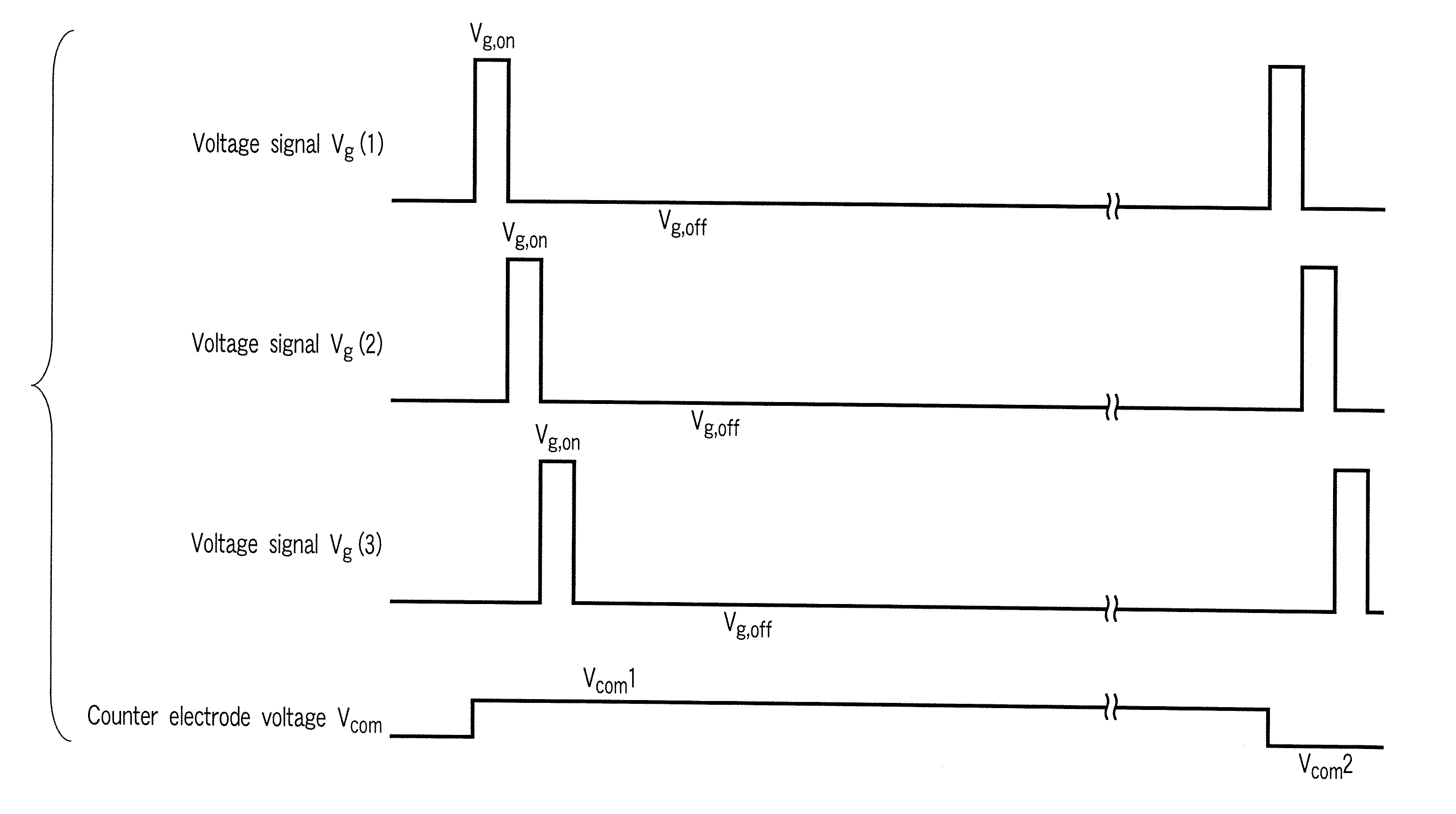
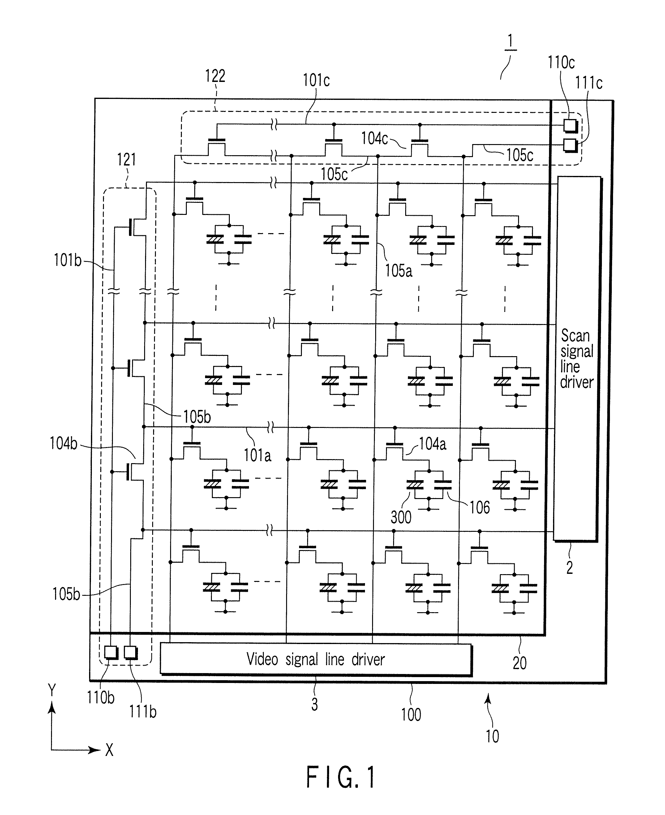
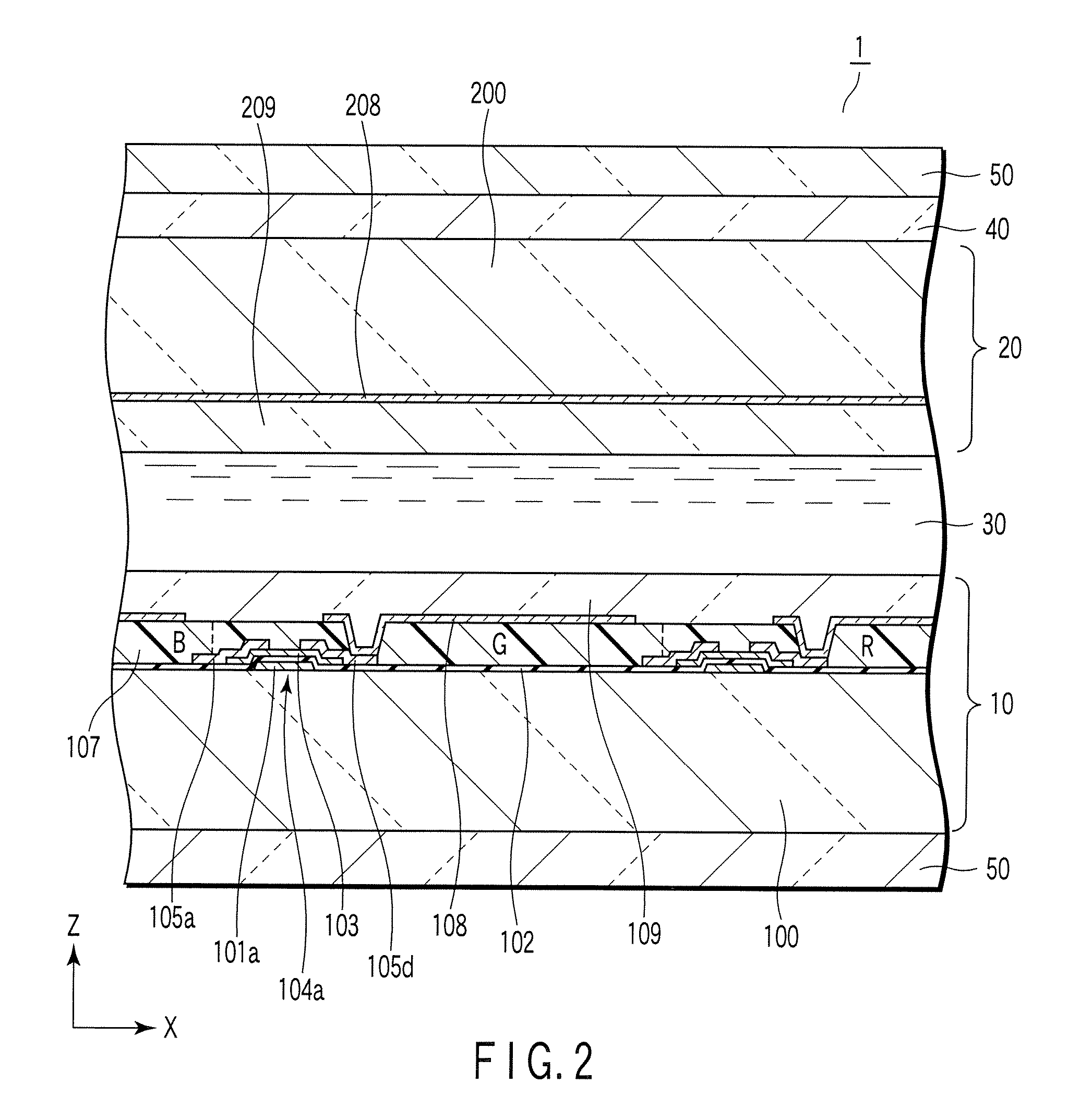
[0097] In this example, the liquid crystal display shown in FIG. 1 was manufactured by the following method. Note that in this embodiment, substantially the same structures as shown in FIG. 7 were used as an array substrate 10 and counter substrate 20.
[0098] In the manufacture of the array substrate 10, scanning lines 101a, reference lines (not shown), and lines 101c and 101b were first formed on a glass substrate 100. Chromium was used as the material of these lines.
[0099] Then, these lines were covered with an insulating film 102 having a layered structure including a chromium oxide film and silicon oxide film. A semiconductor layer 103 made of amorphous silicon was formed on the insulating film 102, and patterned. After that, channel protection layers (not shown) made of silicon nitride were formed on the semiconductor layers 103, and ohmic layers (not shown) were formed on the semiconductor layers 103 and channel protection layers.
[0100] On the insulating film 102, signal lin...
example 2
[0113] A liquid crystal cell was manufactured following the same procedures as explained in Example 1 except that a mixture of UCL-001 (an acrylate monomer having only one acrylic double bond in a molecule) as a liquid crystalline monofunctional acrylate monomer and KAYARAD HX-220 (manufactured by Nippon Kayaku) as a multifunctional acrylate monomer (an acrylate monomer having a plurality of acrylic double bonds in a molecule) having no liquid crystal properties was used as the high-molecular material precursor. As the mixture injected into the empty cell, a mixture containing 95% of liquid crystal E7, 4.7% of UCL-001, 0.25% of HX-220, and 0.05% of 2,2-dimethoxy-2-phenylacetophenone was used. When this liquid crystal cell was observed with a polarizing microscope, with no voltage being applied, the retardation of the liquid crystal layer 30 was smaller in regions between scanning lines 101a and a counter electrode 208 and in regions between signal lines 105a and the counter electrod...
PUM
 Abstract
Description
Claims
Application Information
 - R&D Engineer
- R&D Manager
- IP Professional
- Industry Leading Data Capabilities
- Powerful AI technology
- Patent DNA Extraction
Browse by: Latest US Patents, China's latest patents, Technical Efficacy Thesaurus, Application Domain, Technology Topic.
© 2024 PatSnap. All rights reserved.Legal|Privacy policy|Modern Slavery Act Transparency Statement|Sitemap