
Micro-electromechanical display backplane and improvements thereof

a micro-electromechanical and backplane technology, applied in static indicating devices, instruments, relays, etc., can solve the problems of disproportionate increase of the likelihood of defective transistors, inability to achieve so-called “passive matrix” display, and limited display size, etc., to achieve similar nonlinear switching output characteristics and low cost

Inactive Publication Date: 2007-01-04
SEERTECH CORP
View PDF11 Cites 54 Cited by
  • Summary
  • Abstract
  • Description
  • Claims
  • Application Information

AI Technical Summary

Benefits of technology

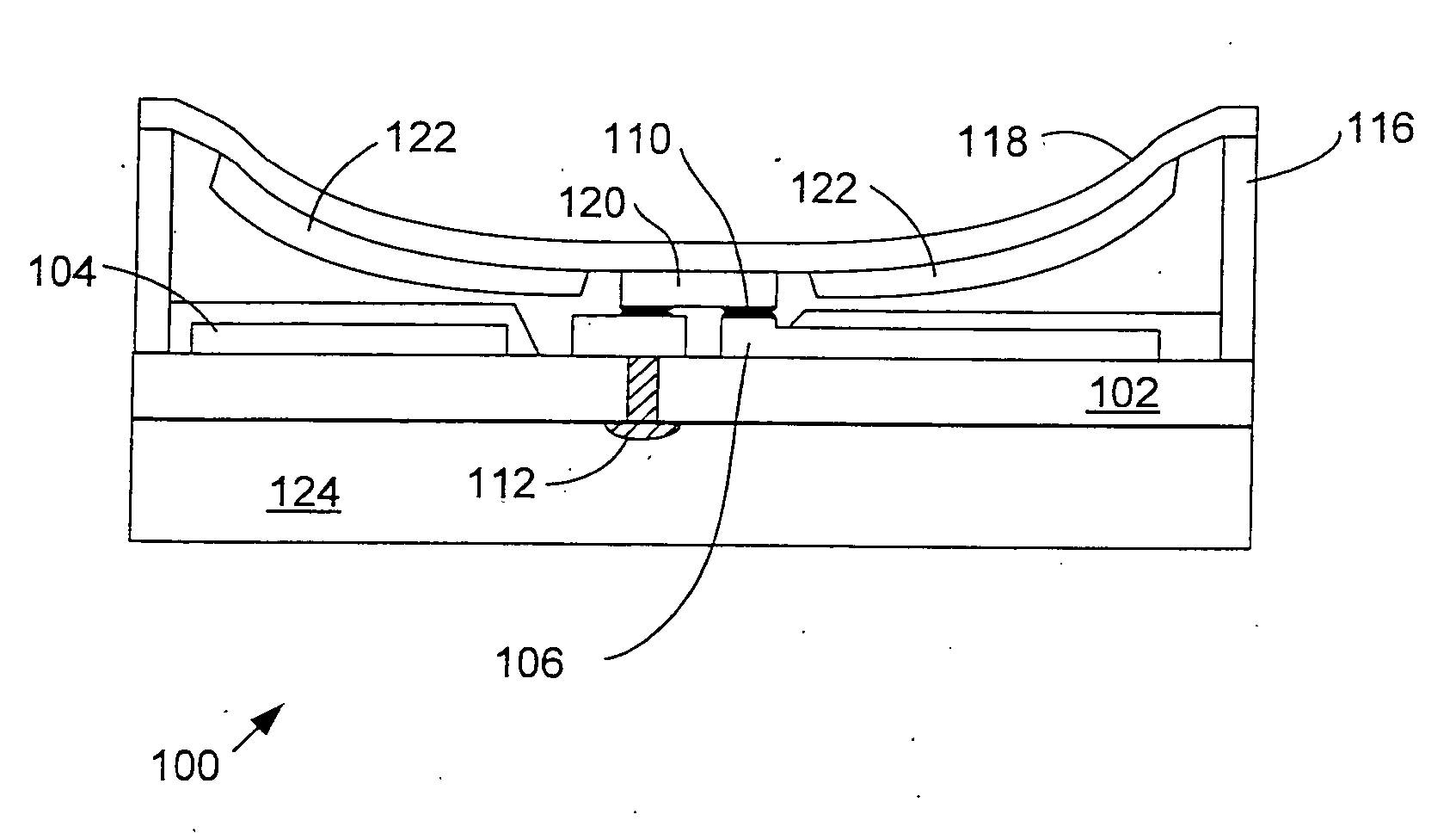
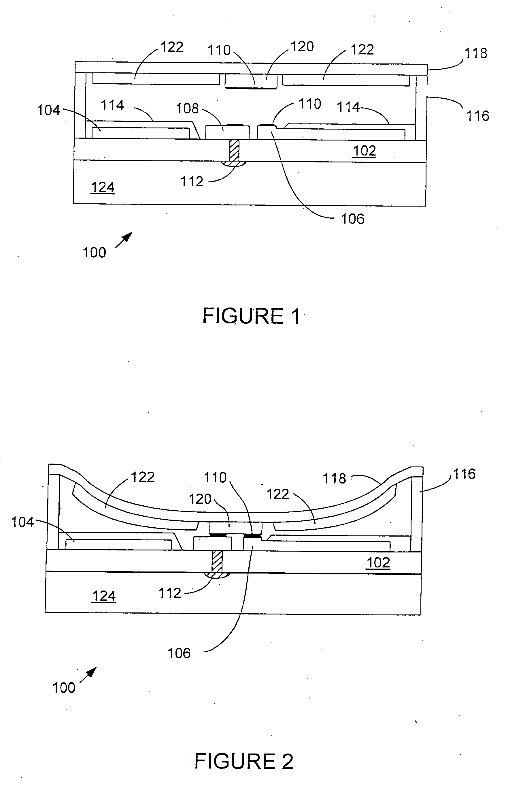
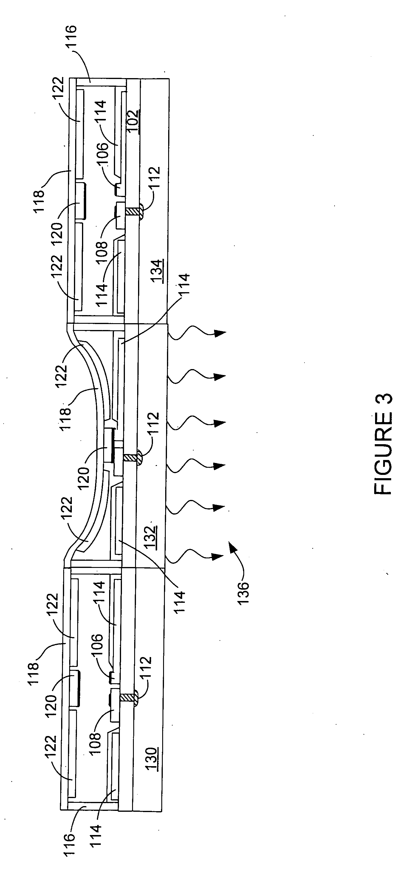
[0014] Embodiments of the present invention provide a matrix of micro electromechanical (MEM) switches that can be manufactured using low cost printing techniques on plastic or other membranes. The MEM switches include a substantially non-pliable membrane and a substantially flexible membrane both of which include electrodes that when energized create electrostatic forces that attracts the flexible membrane to the non-pliable membrane. The matrix of MEM switches can be incorporated into the backplane structure of an optical display. Advantageously, the MEM switches can create similar nonlinear switching output characteristics to the semiconductor-based “active matrix” backplane.
[0016] Embodiments of he MEM switches herein described can be simple to manufacture and of good quality in operation. To improve the operational lifetime of the switches; it is herein also disclosed that there are several mechanisms involving materials selection and electrical interface design that significantly increase the lifetime over what would be expected from common practice. It is by the combination of the switch design, and the associated reliability improvements that this electromechanical backplane design is reliable and inexpensive to manufacture.
[0017] One embodiment of the present invention provides a low cost, scalable backplane for optical displays. The backplane preferably comprises a multi-membrane plastic structure on which is patterned row and column drivers to form the matrix of electromechanical micro switches. Each switch controls the state of a pixel in the optical display device. Critical to successful long-term operation, the present invention includes the application of control voltages to each switch so that the display functions correctly and display life is maximized. With the present invention, it is possible to replace the silicon-on-glass thin film transistors based backplanes with a matrix of MEM switches that are readily manufactured at low process temperatures and with inexpensive equipment. Further, the present invention enables the manufacture of scalable large optical displays on plastic membranes at low cost. Further still, the present invention enables the manufacture of optical displays that may be flexed or twisted into novel shapes while still maintaining the display properties.
[0021] Embodiments of the present invention provide a latching electrostatic display backplane that is combined with electrophoretic material that has a long persistence once set to a given state. This combination provides a flexible electrophoretic display with the best features of paper and traditional electronic display devices. The latching electrostatic display backplane provides unexpected and desirable benefits when used in conjunction with display materials that take a significant amount of time (>30 ms) to transition from one display state to another.
[0022] In a broad sense, the present invention provides a flexible electrophoretic display. One aspect of the present invention provides an improved low-cost, flexible, and useful electrophoretic display assembly and method of manufacturing the electrophoretic display assembly. In one embodiment, the display assembly comprises: a flexible substrate; an electrical connection formed on the flexible substrate; the electrical connection having first and second contact pads; an electrophoretic display element in electrical communication with the first contact pad; and a control circuit mounted on the flexible substrate and in electrical communication with the second contact pad.
[0024] The present invention, in one embodiment, provides co-location of display elements and control circuitry on a shared, flexible substrate. This permits manufacturing of a flexible panel display. In one embodiment, use of an electrophoretic display medium, in particular an encapsulated electrophoretic display material, leads to a flexible display that can be substantially flexed without substantial detrimental impact on the optical performance of the display medium.

Problems solved by technology

Were this not the case, the so-called “Passive Matrix” display would not be possible.
While optical display technology is constantly evolving, the size of the display has been limited by manufacturing problems associated with creating larger and denser backplanes.
Specifically, as the number of thin film transistors on a backplane increase, the likelihood of defective transistors increases disproportionately so manufacturers are forced to invest heavily in developing and procuring semiconductor processing equipment.
Indeed, manufacturing process for large format optical displays suffers a high percentage of rejects due to non-functional transistors.
Because of the poor yield, the consumer is burdened with high pricing for flat screen optical displays.
To improve yields, manufacturers must spend ever-increasing amounts of capital to purchase expensive precision equipment to manufacture the silicon thin film transistors to satisfy the need for large format displays but there is little profit margin so there is no incentive to reduce the pricing to the consumer.
In large-scale optical displays, the backplane accounts for a significant portion of the overall manufacturing cost of the display because of the costs associated with manufacturing the transistor and capacitor matrix.
Additional cost is associated with the membrane, which for virtually all such display backplanes is glass.
Glass, unfortunately, is heavy, non-pliable and prone to breakage.
To reduce weight, the thickness of the glass has been reduced with each succeeding generation of products but as the thickness is reduced, there is a significant negative impact on manufacturing yield with breakage of the glass membrane approaching 50% during the manufacture process.
While plastic membranes are known, it is not a simple task to manufacture silicon transistors on a plastic membrane, primarily because plastic is not well suited to the high process temperatures associated with manufacturing silicon thin film transistors.
Thus, plastic backplanes have not proven to be economically successful, when the manufacturing process is based upon straightforward variations of silicon-on-glass manufacturing technology.
Further, the reliability of prior art silicon-on-plastic backplanes has been poor.
While many consumers desire large format displays, the cost to manufacture large silicon-on-glass backplanes using new tools, such as the commonly referred to Generation 6 fab, is high.
While these tools are able to manufacture backplanes on 35″ glass plates, economies of scale do not offset the reduction in manufacturing yields.
The result is an industry with high capital expenditures, low profit margins and high consumer costs.
Although traditional paper-based media has been used for centuries because of the relative ease of use and low cost, prior art display technology is ill-suited to replace the simple piece of paper.
Unfortunately, once printed on paper, the content cannot be changed thereby limiting paper's useful life.
Traditional electronic displays, such as an LCD display, by contrast, are rigid and inconvenient to carry around, but the contents can be updated constantly by a variety of information sources.
Unfortunately, prior art implementations of these displays have suffered from slow refresh rates, a problem exasperated by design limitations that require a relatively long period between image updates.
This problem is caused by the dynamic memory structure of a typical active matrix display backplane that tends to lose the scan information in a small fraction of a second.
Another problem caused by the dynamic memory structure of the prior art backplane is that the drive power, supplied to update the display elements, gradually decays within the time of a single scan period.
Because of the requirement to multiplex power to each pixel and the fact that the pixels begin to lose the information as soon as the scan of a particular column is complete, the display is very slow to respond to state changes.
The combination of viscous liquid fill materials and the fact that a conventional active matrix backplane can only create an electrostatic field for display material transition for a portion of the time that the display is being scanned makes for slow image updates and an unsatisfactory product.
Another problem with typical active matrix display backplanes arises from the need to use a rigid backing or support structure to carry the thin film transistors that drive the pixels.
Typically, this rigid backing is a piece of glass that is not sufficient flexible enough to bend or flex.
This approach has cost and reliability disadvantages.

Method used


Image

  • Micro-electromechanical display backplane and improvements thereof
  • Micro-electromechanical display backplane and improvements thereof
  • Micro-electromechanical display backplane and improvements thereof

Examples


Embodiment Construction

[0014] Embodiments of the present invention provide a matrix of micro electromechanical (MEM) switches that can be manufactured using low cost printing techniques on plastic or other membranes. The MEM switches include a substantially non-pliable membrane and a substantially flexible membrane both of which include electrodes that when energized create electrostatic forces that attracts the flexible membrane to the non-pliable membrane. The matrix of MEM switches can be incorporated into the backplane structure of an optical display. Advantageously, the MEM switches can create similar nonlinear switching output characteristics to the semiconductor-based “active matrix” backplane.

[0015] In one embodiment the MEM switches include a “latching” mechanism such that once closed, the switch will remain in a closed state until instructed to release the state, thereby allowing for displays that do not require continuous and power wasting refreshing. The mechanism of the switch activation inv...


PUM


Abstract

A low cost, scalable backplane for electrophoretic displays comprising a multi-membrane plastic array of micro electromechanical (MEM) switches. Each switch controls the state of a pixel in the electrophoretic display device. Each switch may be latched to eliminate the need to constantly refresh the device and each switch may function as an enunciator

Description

CROSS-REFERENCES TO RELATED APPLICATIONS [0001] This application is a continuation in part and claims the benefit of commonly assigned non-provisional patent application entitled “ELECTROMECHANICAL ACTIVE DISPLAY BACKPLANE AND IMPROVEMENTS THEREOF” by Michael Sauvante et al, application Ser. No. 10 / 959,604, filed Oct. 5, 2004 and also claims the benefit of commonly assigned U.S. Provisional Application No. 60 / 656,855, filed Feb. 25, 2005 entitled MICRO-ELECTROMECHANICAL SWITCH and U.S. Provisional Application No. 60 / 561,821, filed Apr. 13, 2004 entitled USE OF LONG PERSISTENCE ELECTROPHORETIC DISPLAY MATERIALS ON ACTIVE MATRIX SUBSTRATES, all of which are incorporated herein by reference in its entirety.BACKGROUND OF THE INVENTION [0002] 1. Field of the Invention [0003] Embodiments of the present invention relate to optical display devices. More particularly, embodiments of the present invention relate to a low cost flat panel or electrophoretic display having a micro-electromechani...

Claims


Application Information

Patent Timeline
IPC IPC(8): G09G3/34
CPCG02B26/0841G06F3/0412G09G3/3216G09G3/3266G09G3/3275H01H2001/0063G09G3/3622G09G3/3681G09G3/3692G09G2300/06H01H59/0009G09G3/344G06F3/047
Inventor PASCH, NICHOLAS F.SANDERS, GLENN C.
Owner SEERTECH CORP
Learn More