Semiconductor memory device

a memory device and semiconductor technology, applied in the field of semiconductor memory devices, can solve the problem of detecting a minute bit line leak in one of the pair of bit lines, and achieve the effect of increasing the chip size and detecting the minute bit line leak

Inactive Publication Date: 2007-01-04
FUJITSU MICROELECTRONICS LTD
View PDF5 Cites 16 Cited by
  • Summary
  • Abstract
  • Description
  • Claims
  • Application Information

AI Technical Summary

Benefits of technology

[0012] It is an object of the present invention to provide a semiconductor memory device capable of easily detecting a minute bit line leak without an increase in chip size.

Problems solved by technology

Consequently, erroneous data is read by a read operation, so that a minute bit line leak in the one of the pair of bit lines can be detected.

Method used


Image

  • Semiconductor memory device
  • Semiconductor memory device
  • Semiconductor memory device

Examples


Embodiment Construction

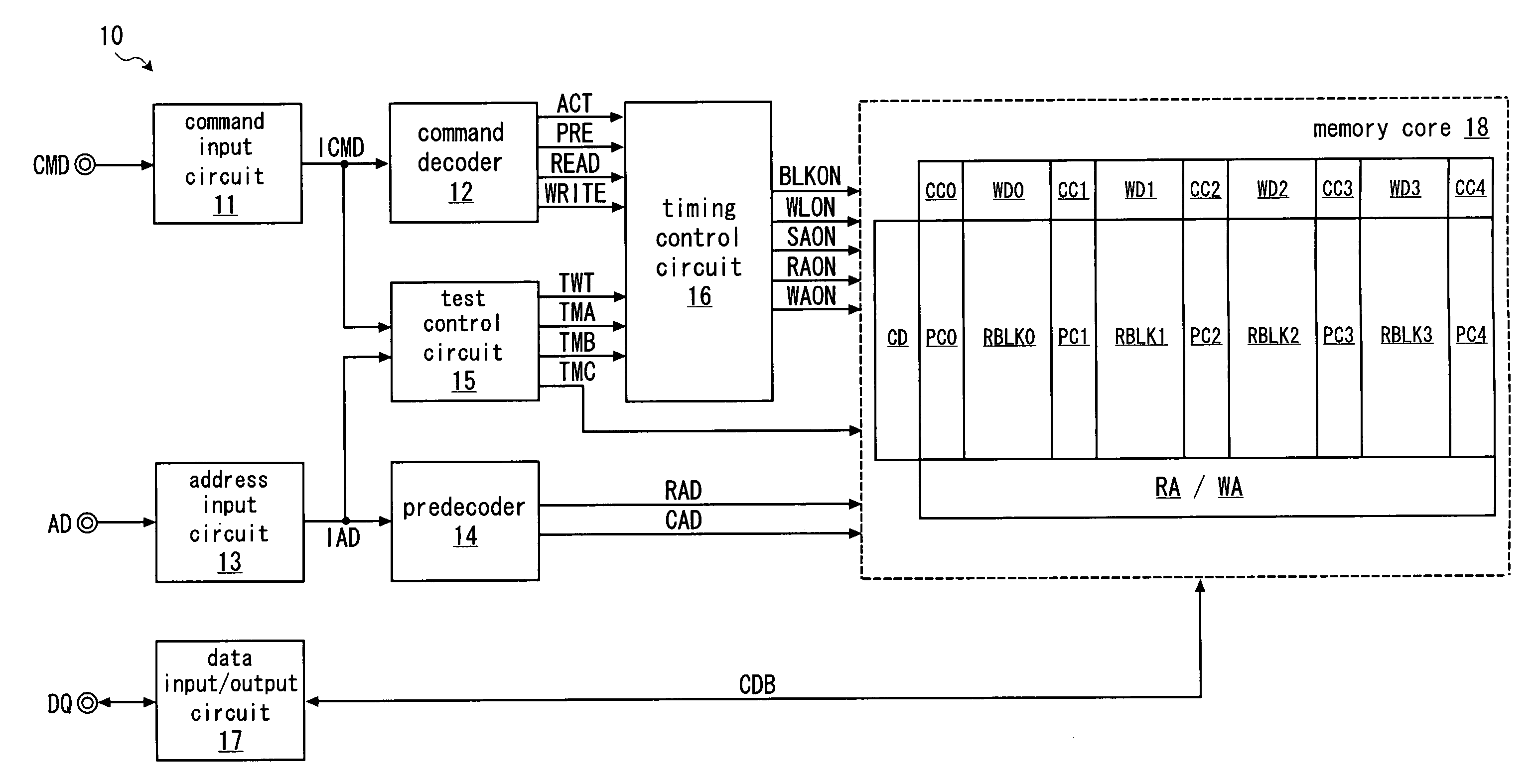
[0030] Hereinafter, an embodiment of the present invention will be described, using the drawings. Note that each terminal and a signal supplied via the terminal are denoted by the same reference symbol. Each signal line and a signal supplied to the signal line are denoted by the same reference symbol. Each voltage line and a voltage supplied to the voltage line are denoted by the same reference symbol. Each signal whose signal name does not have “ / ” at its head is a signal with positive logic, and each signal whose signal name has “ / ” at its head is a signal with negative logic.

[0031]FIG. 1 shows an embodiment of a semiconductor memory device of the present invention. A semiconductor memory device 10, which is formed as, for example, a DRAM, includes a command input circuit11, a command decoder 12, an address input circuit 13, a predecoder 14, a test control circuit 15, a timing control circuit 16, a data input / output circuit 17, and a memory core 18. The command input circuit 11 r...


PUM


Abstract

An equalizing circuit connects a pair of bit lines to each other in response to the activation of an equalizing control signal and connects the pair of bit lines to a precharge voltage line. An equalizing control circuit deactivates the equalizing control signal in response to the activation of a first timing signal. A word line driving circuit activates one of word lines in response to the activation of a second timing signal. A first signal generating circuit of a timing control circuit generates the first timing signal. A second signal generating circuit of the timing control circuit activates the second timing signal after the deactivation of the equalizing control signal accompanying the activation of the first timing signal. A delay control circuit of the second signal generating circuit delays an activation timing of the second timing signal in a test mode from that in a normal mode.

Description

CROSS REFERENCE TO RELATED APPLICATION [0001] This application is based upon and claims the benefit of priority from Japanese Patent Application No. 2005-190298, filed on Jun. 29, 2005, the entire contents of which are incorporated herein by reference. BACKGROUND OF THE INVENTION [0002] 1. Field of the Invention [0003] The present invention relates to a semiconductor memory device, and more particularly, to a testing technique for detecting a bit line leak in a semiconductor memory device. [0004] 2. Description of the Related Art [0005] In a semiconductor memory device such as a DRAM (Dynamic Static Random Access Memory), if a bit line leak occurs due to, for example, a short-circuit between a bit line and a word line, erroneous data is sometimes read through a read operation as described below. While the semiconductor memory device is in a standby state, an equalizing control signal to an equalizing circuit is activated. The equalizing control circuit connects a pair of bit lines t...

Claims


Application Information

Patent Timeline
Patent Type & Authority Applications(United States)
IPC IPC(8): G11C29/00
CPCG11C11/401G11C29/025G11C29/02G11C7/12G11C7/22G11C8/08G11C11/4076G11C11/4085G11C11/4094
Inventor IKEDA, HITOSHIMORI, KAORUOKUYAMA, YOSHIAKI
Owner FUJITSU MICROELECTRONICS LTD
Why Eureka
Try Eureka