Semiconductor device

a technology of semiconductor film and dielectric film, which is applied in the direction of semiconductor device, semiconductor/solid-state device details, electrical apparatus, etc., can solve the problems of more deterioration in the mechanical and more deterioration in the bonding strength of the low-k film

Inactive Publication Date: 2007-01-11
KK TOSHIBA
View PDF2 Cites 12 Cited by
  • Summary
  • Abstract
  • Description
  • Claims
  • Application Information

AI Technical Summary

Benefits of technology

[0010] According to yet another aspect of the invention, there is provided a semiconductor device comprising: a plurality of inter-level dielectric films which are stacked and provided in plural layers above a substrate; at least one lower layer conductor which is provided in at least one inter-level dielectric film of the stacked inter-level dielectric films; and at least one first conductor which is electrically unconnected to the lower layer conductor and which is provided in an inter-level dielectric film above the inter-level dielectric film in which the lower layer conductor is provided at the position above the lower layer conductor and overlapping the lower layer conductor partly, at least a part of the first conductor having a smaller line width at the position off the area above the lower layer conductor and, at this position, passing through the inter-level dielectric film above the inter-level dielectric film in which the lower layer conductor is provided along the film thickness direction thereof.

Problems solved by technology

As a result, the mechanical strength of a material itself is deteriorated (decreased) in the low-k film more than in a commonly-used dielectric film.
Further, in so-called a low-k inter-level dielectric film obtained by stacking a plurality of low-k films, the bonding strength is deteriorated (decreased) at the interface between stacked low-k films or at the interface between the low-k film and other dielectric film is deteriorated (decreased) more than at the interface between commonly used dielectric films.
The deterioration in the mechanical strength of the low-k film and the deterioration in the bonding strength at the interface between the low-k films or at the interface between the low-k film and other dielectric film pose a serious problem in implementing multilayer wiring structure in a semiconductor device as follows.

Method used


Image

  • Semiconductor device
  • Semiconductor device
  • Semiconductor device

Examples


first embodiment

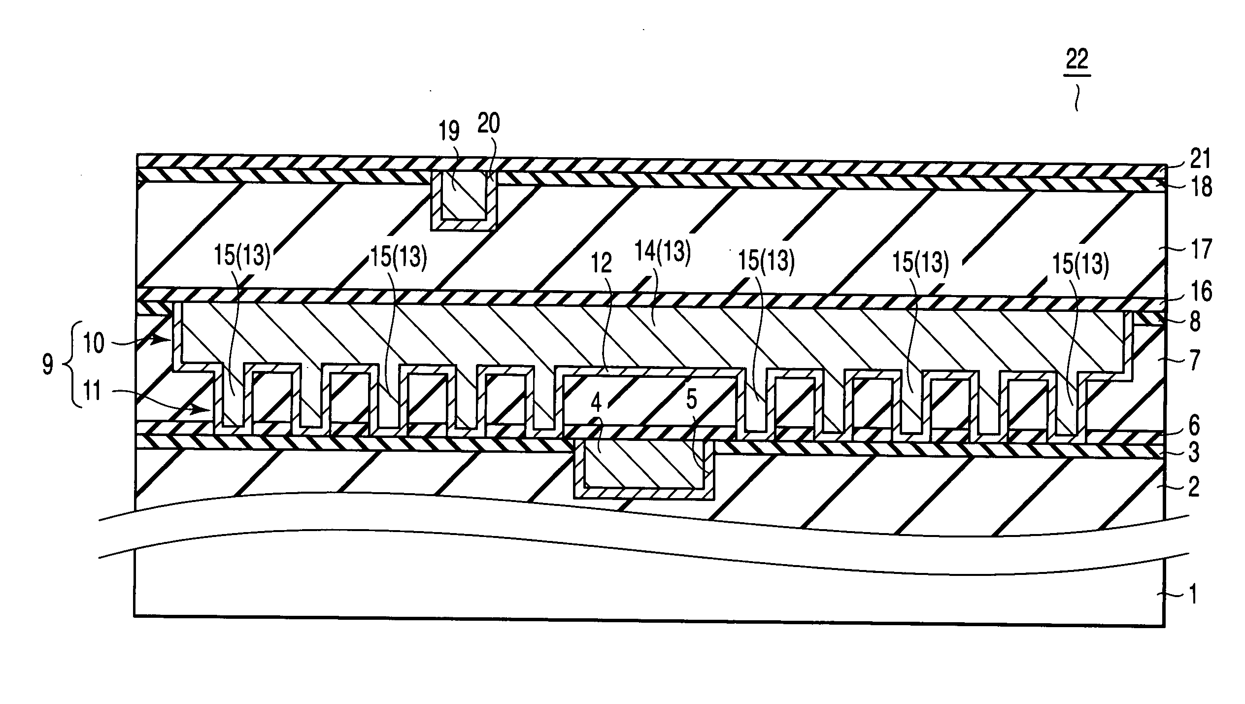
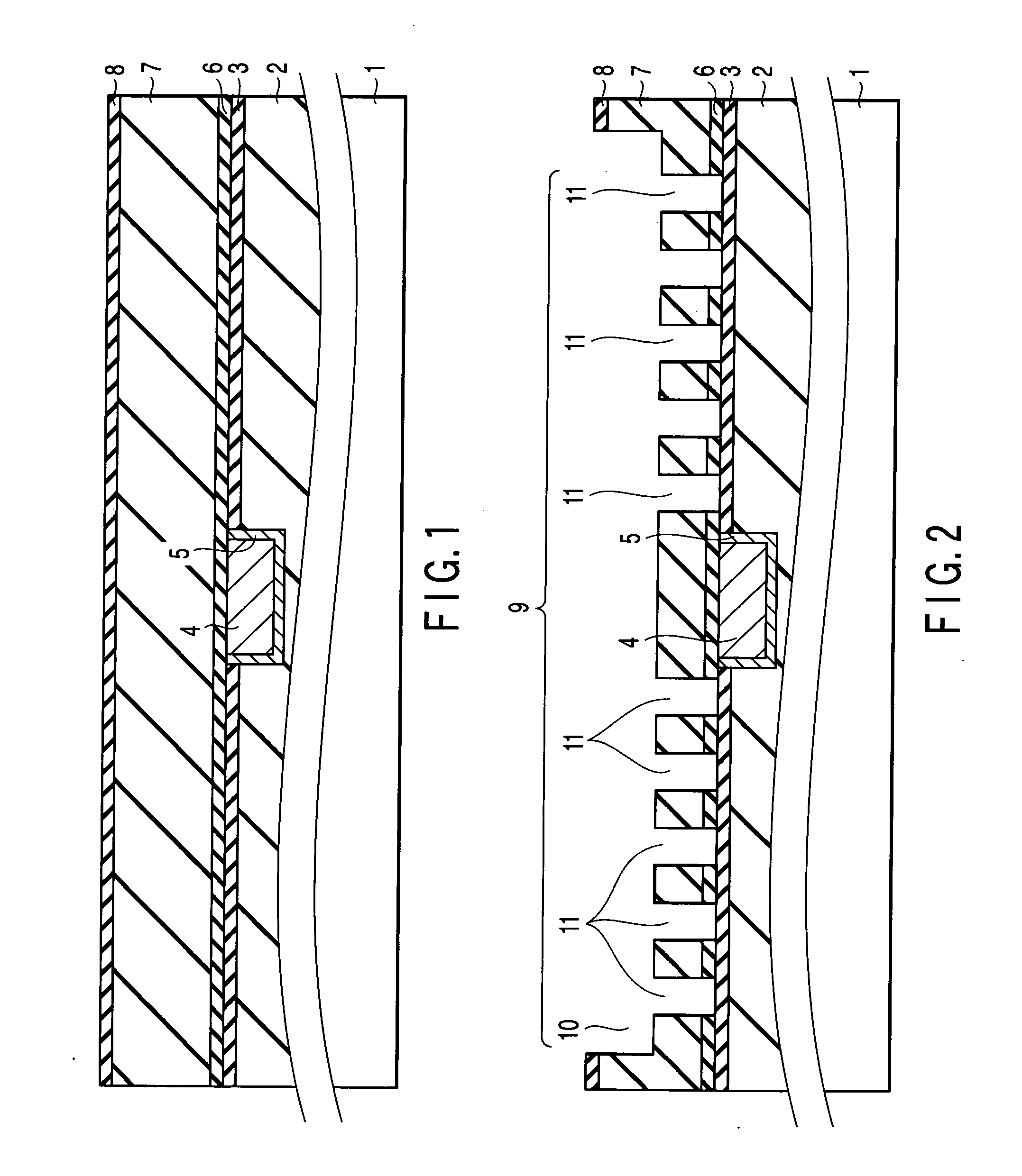
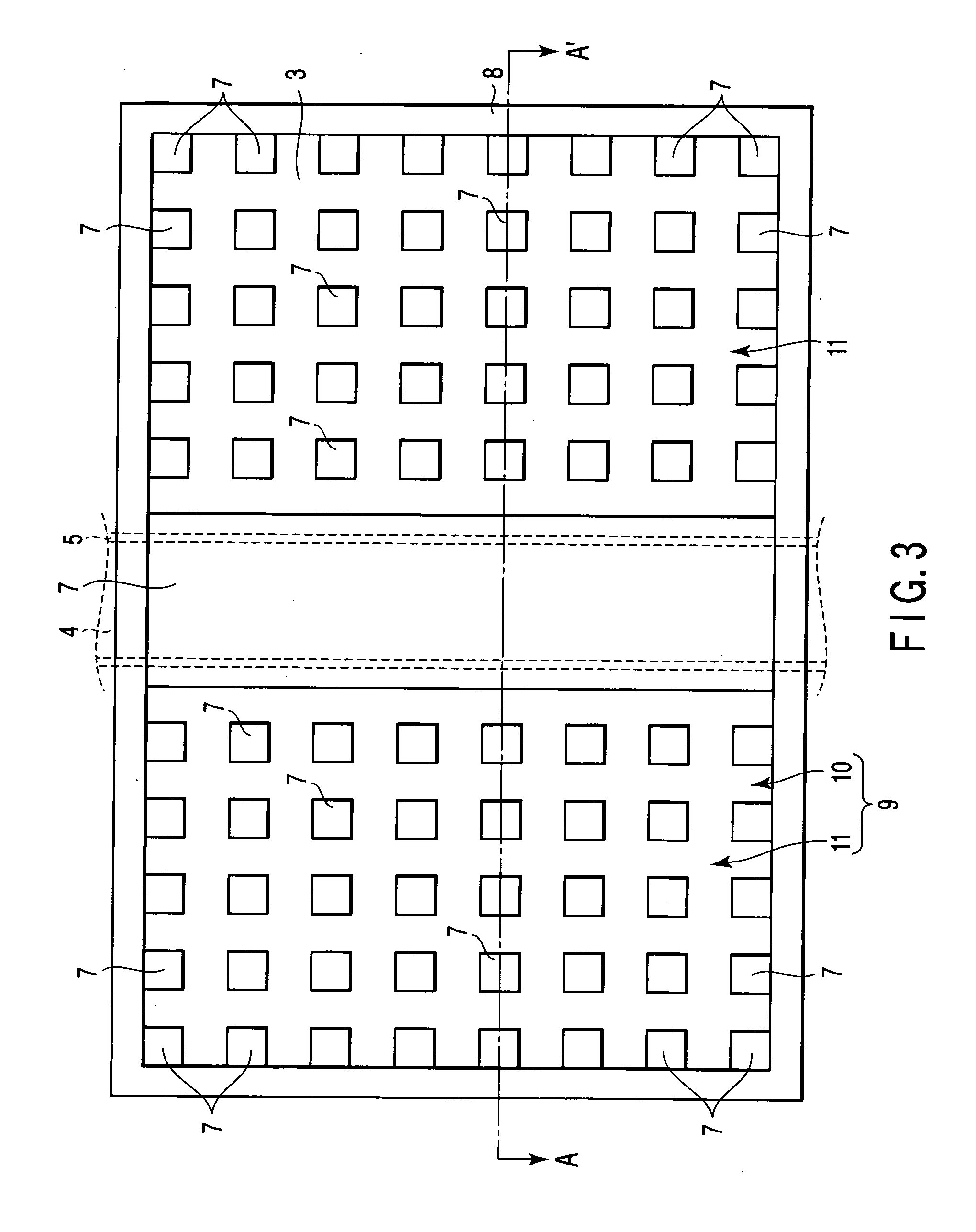
[0035] Firstly, a first embodiment of the present invention will be described with reference to FIGS. 1 to 14. FIG. 14 is a plan view showing a semiconductor device according to the first embodiment, and FIGS. 1 to 13 show a manufacturing process of a semiconductor device according to this embodiment.

[0036] In the first embodiment, a configuration in which sacrificial via plugs to which a current is not supplied actually are provided in succession, on a layer including a lower-side via plug of so-called a broad wiring, along two directions: along the longitudinal direction of the broad wiring and along the direction substantially perpendicular to the longitudinal direction thereof to thereby increase the mechanical strength of the area of the broad wiring will be described. Hereinafter, detailed description will be made.

[0037] Firstly, as shown in FIG. 1, an inter-level dielectric film (ILD) 2 in the (n−1)-th (n is a natural number of 2 or more) layer is formed above a silicon sub...

second embodiment

[0058] A second embodiment of the present invention will next be described below with reference to FIGS. 15 to 17. FIG. 15 is a cross-sectional view showing a semiconductor device serving as a comparison example to the second embodiment. FIG. 16 is a cross-sectional view showing a semiconductor device according to the second embodiment. FIG. 17 is a plan view showing a semiconductor device according to the second embodiment and a semiconductor device serving as a comparison example to the second embodiment. Note that, in the second embodiment, the same reference numerals denote the same or corresponding parts as in the first embodiment, and the detailed description thereof will be omitted.

[0059] In the second embodiment, the mechanical strength of the region near the wiring is increased by extending the wiring to the layer situated on the lower side of the actually used wiring, on which the via plug is formed. Hereinafter, detailed description will be made. The manufacturing proces...

third embodiment

[0070] A third embodiment of the present invention will next be described below with reference to FIGS. 18 and 19. FIG. 18 is a cross-sectional view showing a semiconductor device according to the third embodiment. FIG. 19 is a plan view showing a semiconductor device according to the third embodiment. In the third embodiment, the same reference numerals denote the same or corresponding parts as in the above-described first and second embodiments, and the detailed description thereof will be omitted.

[0071] In the third embodiment, a plurality of lower layer conductors are formed in one layer, and at least one first conductor is extended upward of the plurality of lower layer conductors and formed in an inter-level dielectric film one layer above the layer in which the lower layer conductors are formed. Hereinafter, a semiconductor device 41 according to the third embodiment will be described with reference to FIGS. 18 and 19.

[0072] As shown in FIG. 18, in the semiconductor device ...


PUM


Abstract

There is disclosed a semiconductor device comprising a plurality of inter-level dielectric films which are stacked and provided in plural layers above a substrate, at least one first conductor which is provided in at least one inter-level dielectric film of the stacked inter-level dielectric films, and a plurality of second conductors which are provided in the inter-level dielectric film in which the first conductor is provided and which are connected to the lower surface of the first conductor and which are extended along the downward direction from the first conductor and further extended along a first direction and a second direction perpendicular to the first direction in such a manner as to be spaced apart from each other to form a lattice shape.

Description

CROSS-REFERENCE TO RELATED APPLICATIONS [0001] This application is based upon and claims the benefit of priority from prior Japanese Patent Application No. 2005-198967, filed Jul. 7, 2005, the entire contents of which are incorporated herein by reference. BACKGROUND OF THE INVENTION [0002] 1. Field of the Invention [0003] The present invention relates to a semiconductor device and, more particular, to a technique that increases reliability of a semiconductor device including an inter-level dielectric film made of a low dielectric constant dielectric film. [0004] 2. Description of the Related Art [0005] In recent years, application of a so-called low dielectric constant dielectric film (Low-k film) having a dielectric constant lower than a commonly-used dielectric film and serving as a material of an inter-level dielectric film of a semiconductor device is proceeding in order to speed up the operation speed of the semiconductor device. The low-k film is obtained by, for example, redu...

Claims


Application Information

Patent Timeline
Patent Type & Authority Applications(United States)
IPC IPC(8): H01L29/00
CPCH01L21/76801H01L21/76807H01L21/76816H01L21/76832H01L21/76835H01L23/522H01L2924/0002H01L23/53238H01L23/53295H01L2924/00H01L23/5283
Inventor HASUNUMA, MASAHIKOITO, SACHIYO
Owner KK TOSHIBA
Why Eureka
Try Eureka