

Analog-to-digital converter and semiconductor device
- Summary
- Abstract
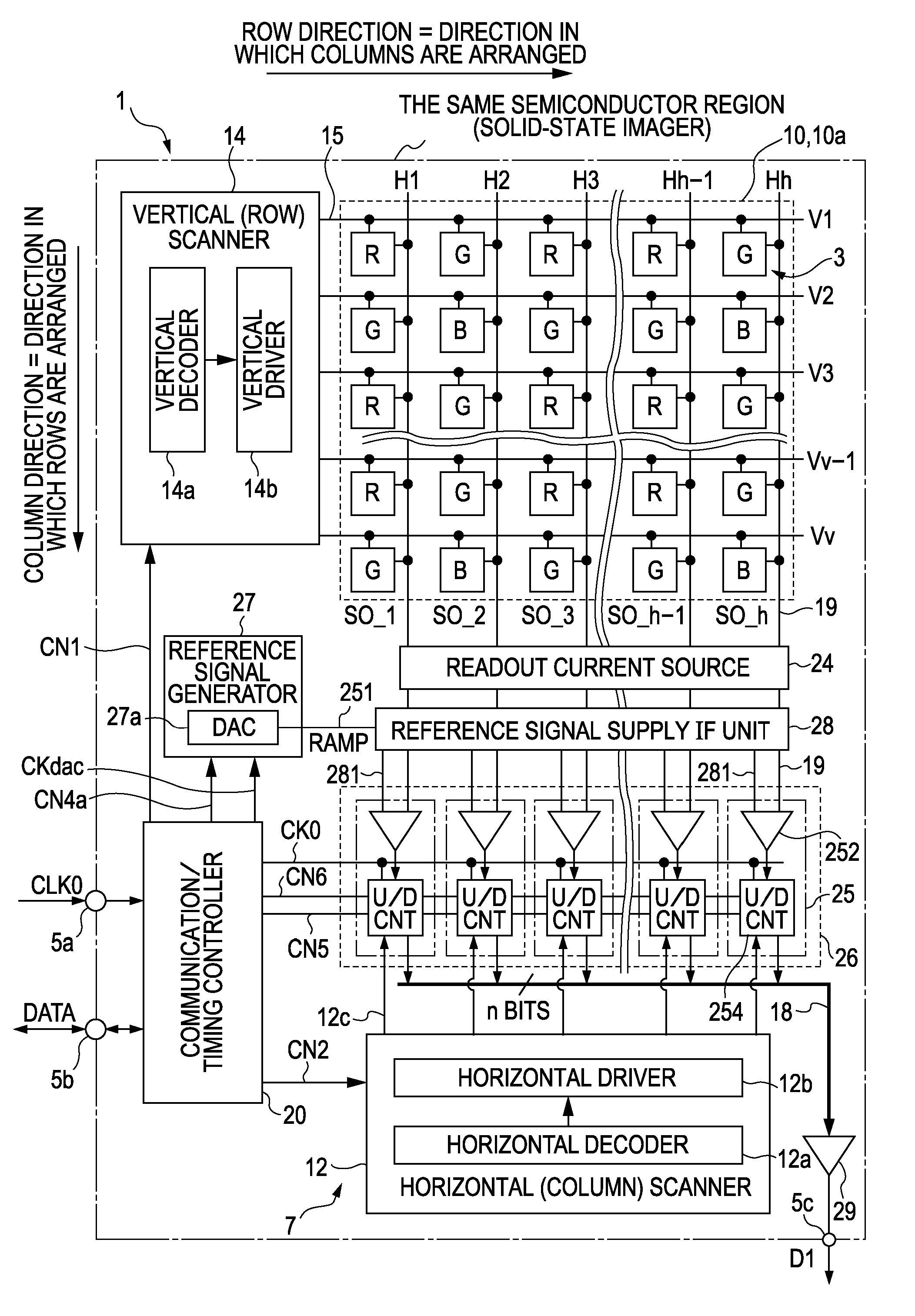
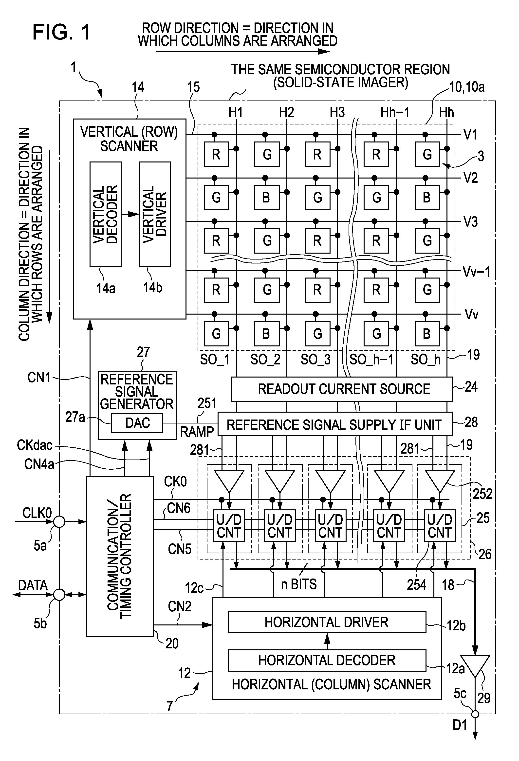
- Description
- Claims
- Application Information
AI Technical Summary
Benefits of technology
Problems solved by technology
Method used
Image

Examples
first embodiment
Buffer Circuit (First Embodiment)
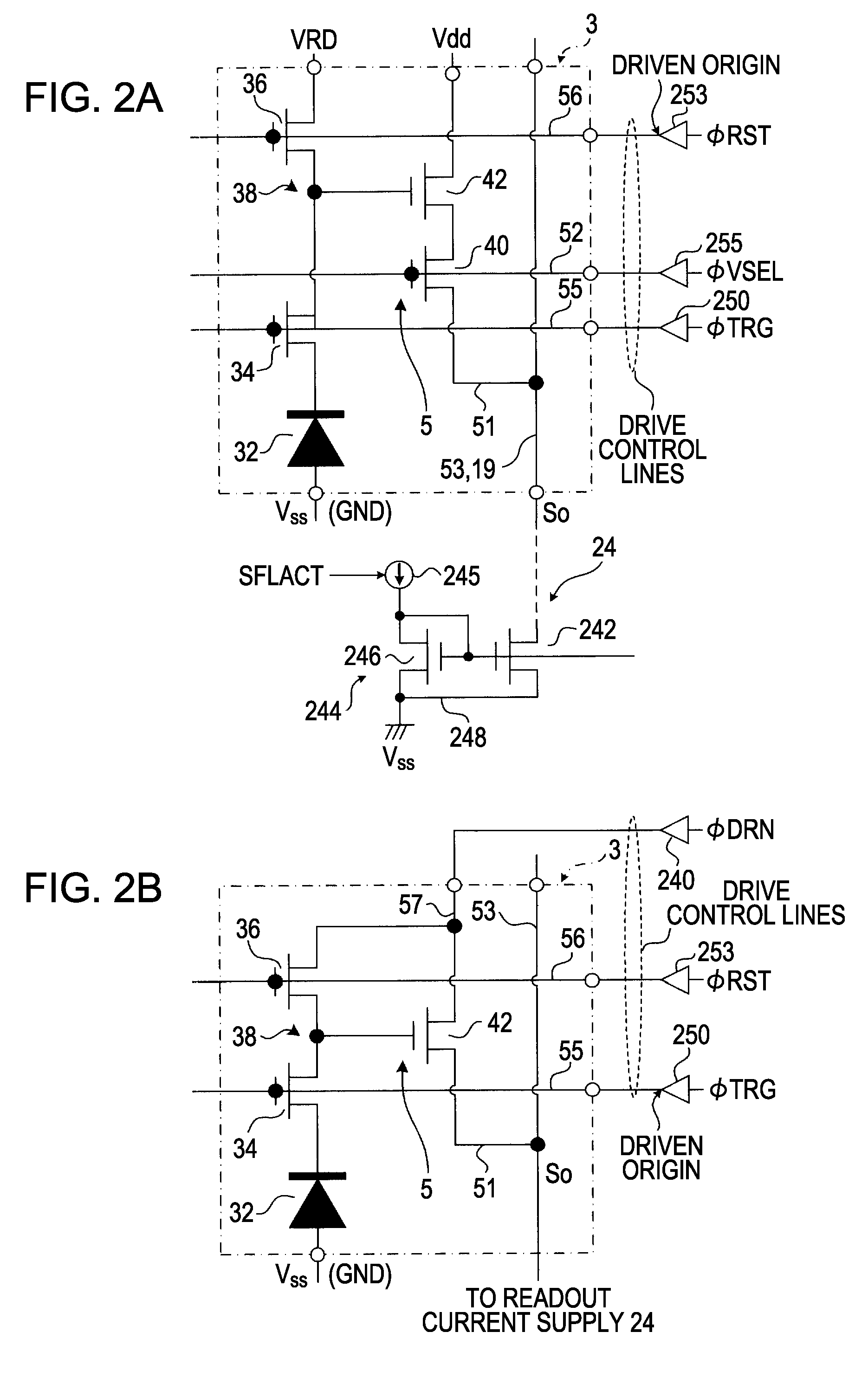
[0192]FIG. 10 is a diagram showing, together with a detailed example of the configuration of the voltage comparator 252, a detailed example of the configuration of the buffer circuit 280 according to the first embodiment. FIG. 11 is a diagram showing, together with a detailed example of the configuration of the voltage comparator 252, a detailed example of the configuration of a known buffer circuit 280 serving as a comparison example.
[0193] The buffer circuit 280 is a source follower circuit. Specifically, the buffer circuit 280 includes an NMOS transistor (referred to as an “amplifying transistor”) 282, which is connected at its drain to the power supply Vdd and which receives at its gate the reference signal RAMP via the reference signal line 251, and an NMOS transistor (referred to as a “load MOS transistor”) 284, which is connected between the source of the amplifying transistor 282 and the ground and which supplies the operating current to the...
second embodiment
Reference Signal Supply IF Unit (Second Embodiment)
[0206]FIGS. 14 and 15 are diagrams showing the reference signal supply IF unit 28 according to the second embodiment. In particular, the signal transmission (interface) among the unit pixels 3, the reference signal generator 27, and the voltage comparators 252 included in the column AD circuits 25 will be examined. FIG. 14 shows the basic configuration of an interface for use in the second embodiment. FIG. 15 shows the overall outline of the interface.
[0207] In the reference signal supply IF unit 28 according to the first embodiment, with the reference-signal-input-stage-separated configuration in which the reference signal input stages of the voltage comparators 252 are separated into a plurality of blocks, one block includes one buffer circuit 280 and a plurality of voltage comparators 252. In other words, the number of voltage comparators 252 covered by one buffer circuit 280 is plural. In contrast, in the second embodiment, one...
PUM
 Abstract
Description
Claims
Application Information