Method and system for deposition tuning in an epitaxial film growth apparatus

a film growth and epitaxial technology, applied in the direction of individual semiconductor device testing, semiconductor/solid-state device testing/measurement, instruments, etc., can solve the problems of increasing manual control of semiconductor film growth process, difficult to maintain and difficult to achieve high level of uniformity. , to achieve the effect of minimizing deviations from the target thickness

Inactive Publication Date: 2007-01-11
APPLIED MATERIALS INC
View PDF10 Cites 56 Cited by
  • Summary
  • Abstract
  • Description
  • Claims
  • Application Information

AI Technical Summary

Benefits of technology

[0006] Embodiments of the invention include a method of calculating a process parameter for a deposition of an epitaxial layer on a substrate. The method includes the steps of measuring an effect of the process parameter on a thickness of the epitaxial layer to determine a gain curve for the process parameter, and calculating, using the gain curve, a value for the process parameter to achieve a target thickness of the epitaxial layer. The value is calculated to minimize deviations from the target thickness in the layer.

Problems solved by technology

Maintaining a high level of uniformity is made even more challenging due to the increasing sizes of the substrates, with the standard substrate wafer diameter moving from 200 mm to 300 mm, and beyond.
In EPI processes for making alloy films (e.g., SiGe films), especially doped alloy films, the sensitivity of several process parameters on film quality is increased, making it more difficult to tune these parameters by hand.
The increased sensitivity makes manual control of semiconductor film growth processes much more difficult, if not impossible.
There is also increasing complexity in the relationship between process parameters and the qualities of the manufactured film layer.
Increasingly, the interdependences of multiple process parameters on a property of the layer make it more difficult to find optimum values for the parameters to achieve a target value for the property.
Moreover, the interdependence of the parameters make determining the parameter values much more difficult than if the effects of each parameter on thickness uniformity were completely independent.

Method used


Image

  • Method and system for deposition tuning in an epitaxial film growth apparatus
  • Method and system for deposition tuning in an epitaxial film growth apparatus
  • Method and system for deposition tuning in an epitaxial film growth apparatus

Examples


Embodiment Construction

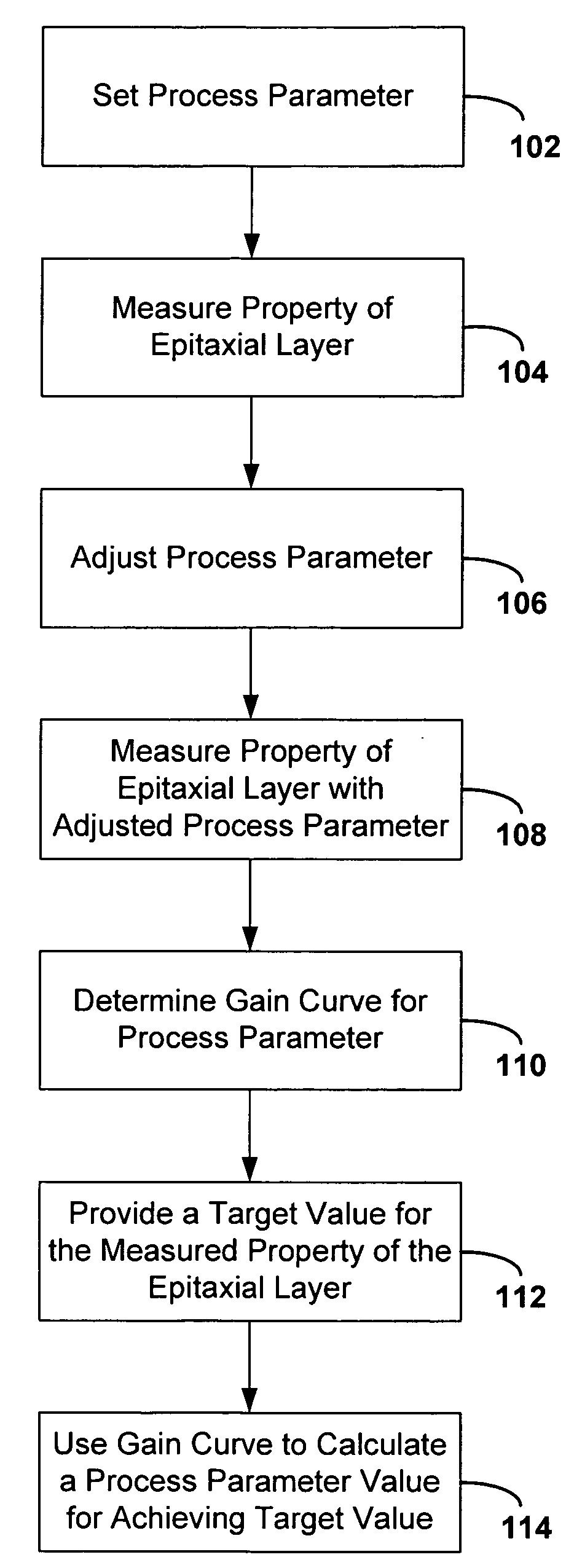
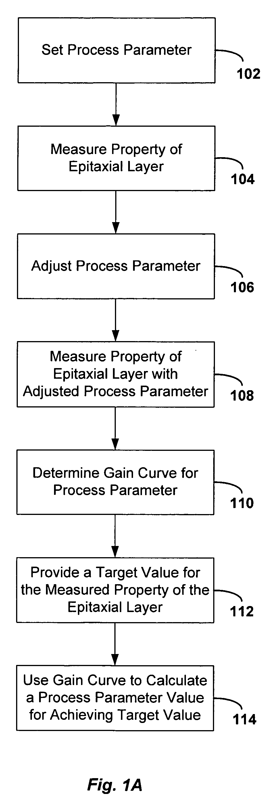
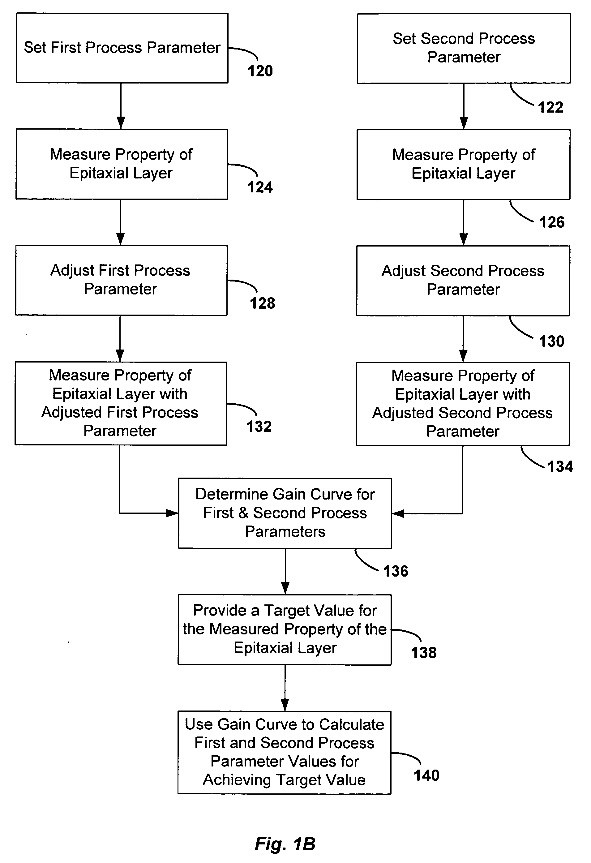
[0019] Methods and systems are described for tuning parameters in an epitaxial film growth process in order to achieve films with a desired thickness uniformity and / or compositional distribution. Tunable process parameters include power settings for heating elements in the various substrate heating zones of the process chamber, and partial pressures and flow rate settings of the process gases used in the chamber, among other parameters.

[0020] The methods include the creation of gain curves and / or algorithms that model the effects of the process parameters on the characteristics of the films. For example, a gain curve may be determined that plots a ratio of the power delivered to heating elements in different substrate heating zones (i.e., the process parameter) against variations in the thickness of the film layer. The gain curve may be used to calculate a power ratio that forms a film layer with minimized variations from a target thickness. Additional aspects of embodiments of the...


PUM

PropertyMeasurementUnit
diameteraaaaaaaaaa
angleaaaaaaaaaa
temperatureaaaaaaaaaa

Abstract

A method of calculating a process parameter for a deposition of an epitaxial layer on a substrate. The method includes the steps of measuring an effect of the process parameter on a thickness of the epitaxial layer to determine a gain curve for the process parameter, and calculating, using the gain curve, a value for the process parameter to achieve a target thickness of the epitaxial layer. The value is calculated to minimize deviations from the target thickness in the layer. Also, a substrate processing system comprising that includes a processor to calculate a value for the process parameter to achieve a substantially uniform epitaxial layer of a target thickness on the substrate, where the value is calculated using a gain curve derived from measurements of layer uniformity as a function of the value of the process parameter.

Description

BACKGROUND OF THE INVENTION [0001] Modern processes for manufacturing semiconductor devices require precise adjustment of many process parameters to achieve high levels of device performance, product yield, and overall product quality. For processes that include the formation of semiconductive layers on substrates with epitaxial film growth, numerous process parameters have to be carefully controlled, including the substrate temperature, the pressures and flow rates precursor materials, the formation time, and the distribution of power among the heating elements surrounding the substrate, among other process parameters. [0002] Current trends in CMOS technology are favoring processes that can produce increasingly thin layers (e.g., dielectric layers only 60-80 Å thick or less), and films with increasing complexity. For example, conventional BiCMOS devices, using single-element silicon (Si) films, are being displaced by two-element, silicon-germanium (SiGe) films that have superior qu...

Claims


Application Information

Patent Timeline
Patent Type & Authority Applications(United States)
IPC IPC(8): H01L21/66H01L21/20
CPCC23C16/52C30B23/02Y10T117/10C30B25/165C30B25/02
Inventor ADERHOLD, WOLFGANG R.ZOJAJI, ALI
Owner APPLIED MATERIALS INC
Why Eureka
Try Eureka