

Probing pads in kerf area for wafer testing
- Summary
- Abstract
- Description
- Claims
- Application Information
AI Technical Summary
Benefits of technology
Problems solved by technology
Method used
Image

Examples
Embodiment Construction
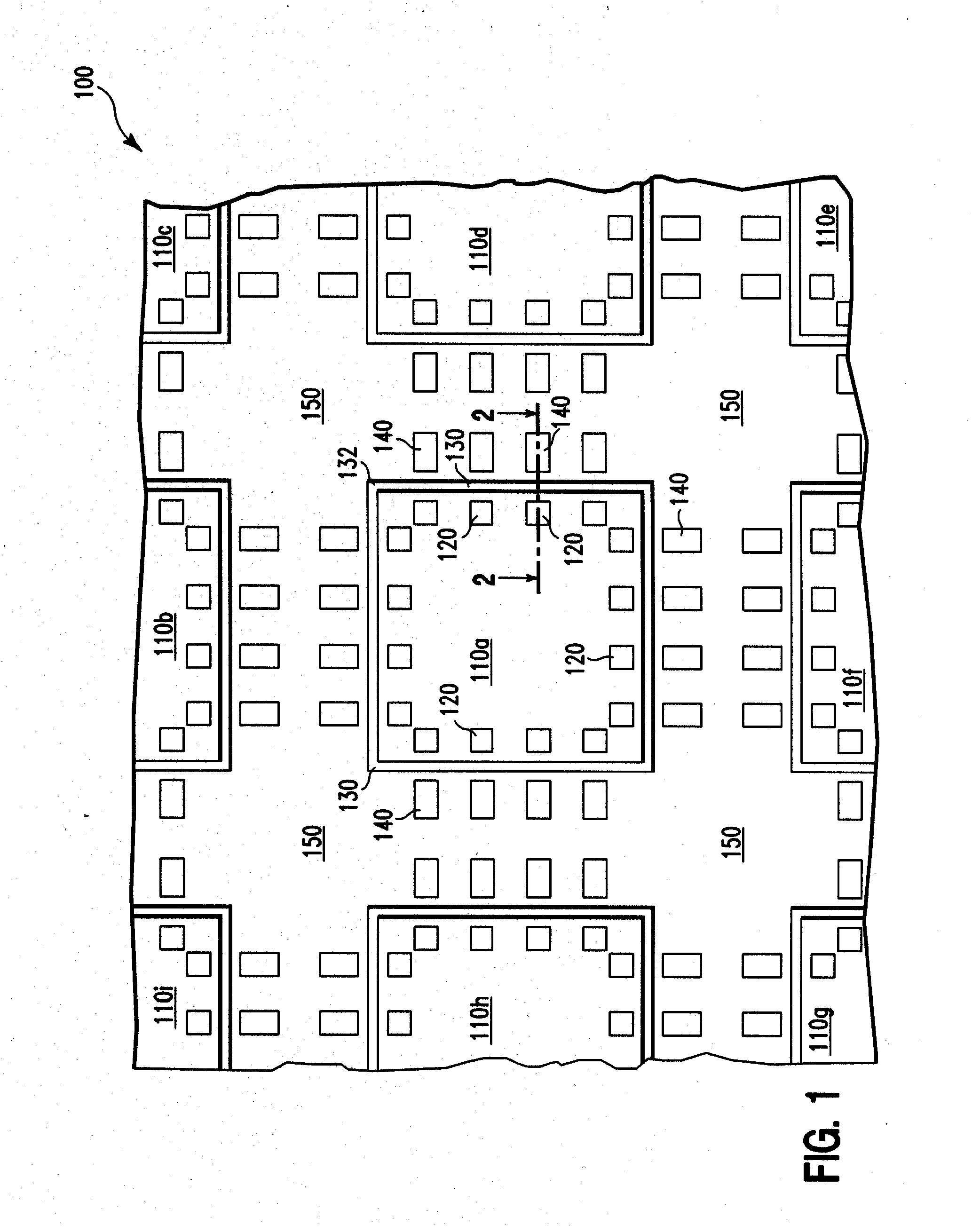
[0012]FIG. 1 illustrates a top down view of a wafer 100, in accordance with embodiments of the present invention. For illustration, the wafer 100 comprises 9 integrated circuits (i.e., chips) 110a-110i and other structures associated with the chips 110a-110i. In general, the wafer 100 can comprise N chips, N being a positive integer. Of the chips 110a-110i, only the chip 110a and its associated structures are fully described and fully shown in FIG. 1. The wafer 100 further comprises a kerf region 150 (i.e., dicing channels) physically separating the chips 110a-11Oi. During chip separation (i.e., chip dicing), in one embodiment, a blade (not shown) can be used to cut along the kerf region 150 so as to separate the chips 110a-110i from each other.
[0013] In one embodiment, the chip 110a comprises, illustratively, 16 bond pads 120 (comprising aluminum in one embodiment) and is surrounded on the chip's perimeter by a protection ring 130. Associated with the chip 110a are 16 probe pads 1...
PUM
 Abstract
Description
Claims
Application Information