Semiconductor device and method of controlling the same
- Summary
- Abstract
- Description
- Claims
- Application Information
AI Technical Summary
Benefits of technology
Problems solved by technology
Method used
Image

Examples
first embodiment
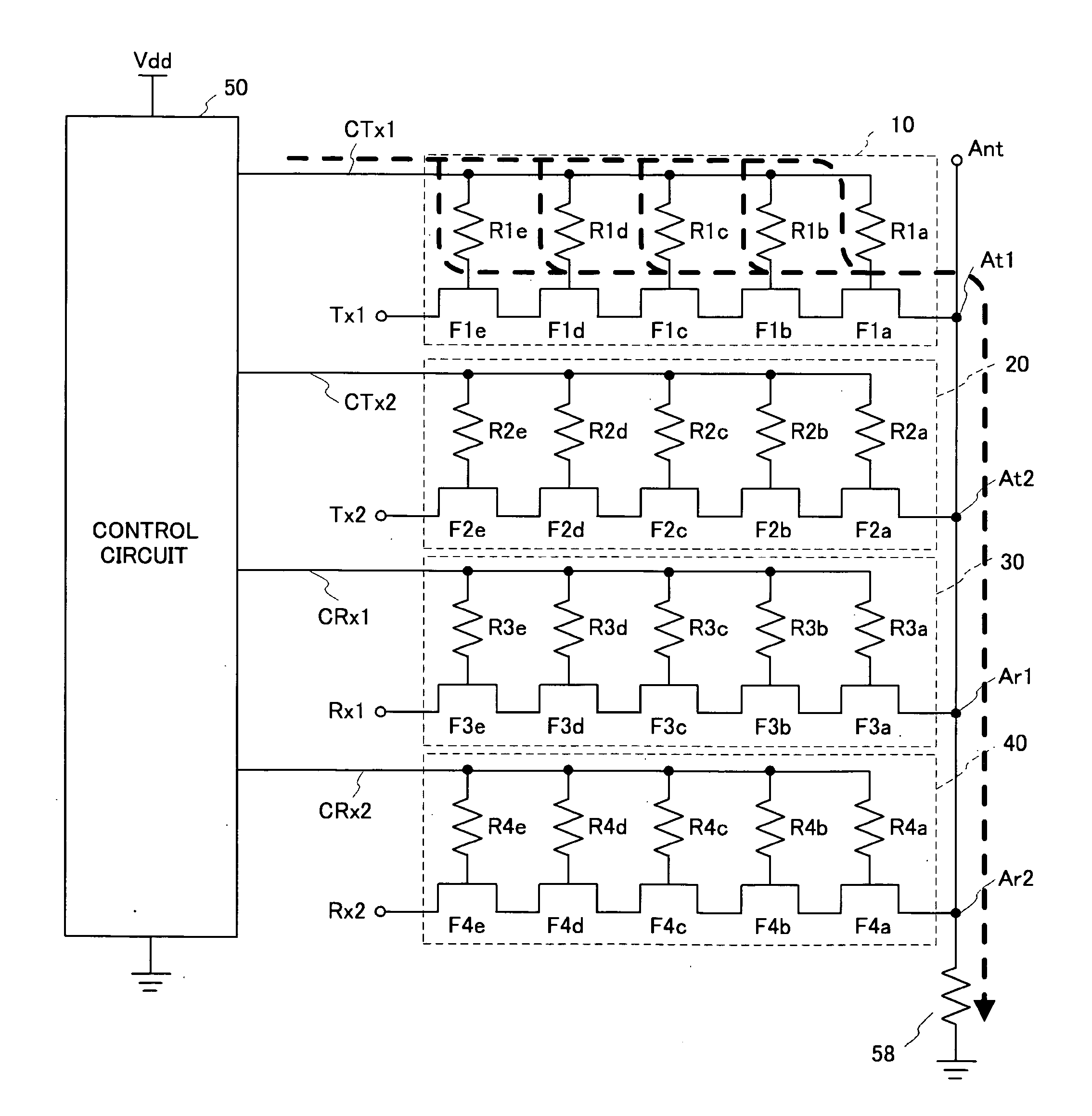
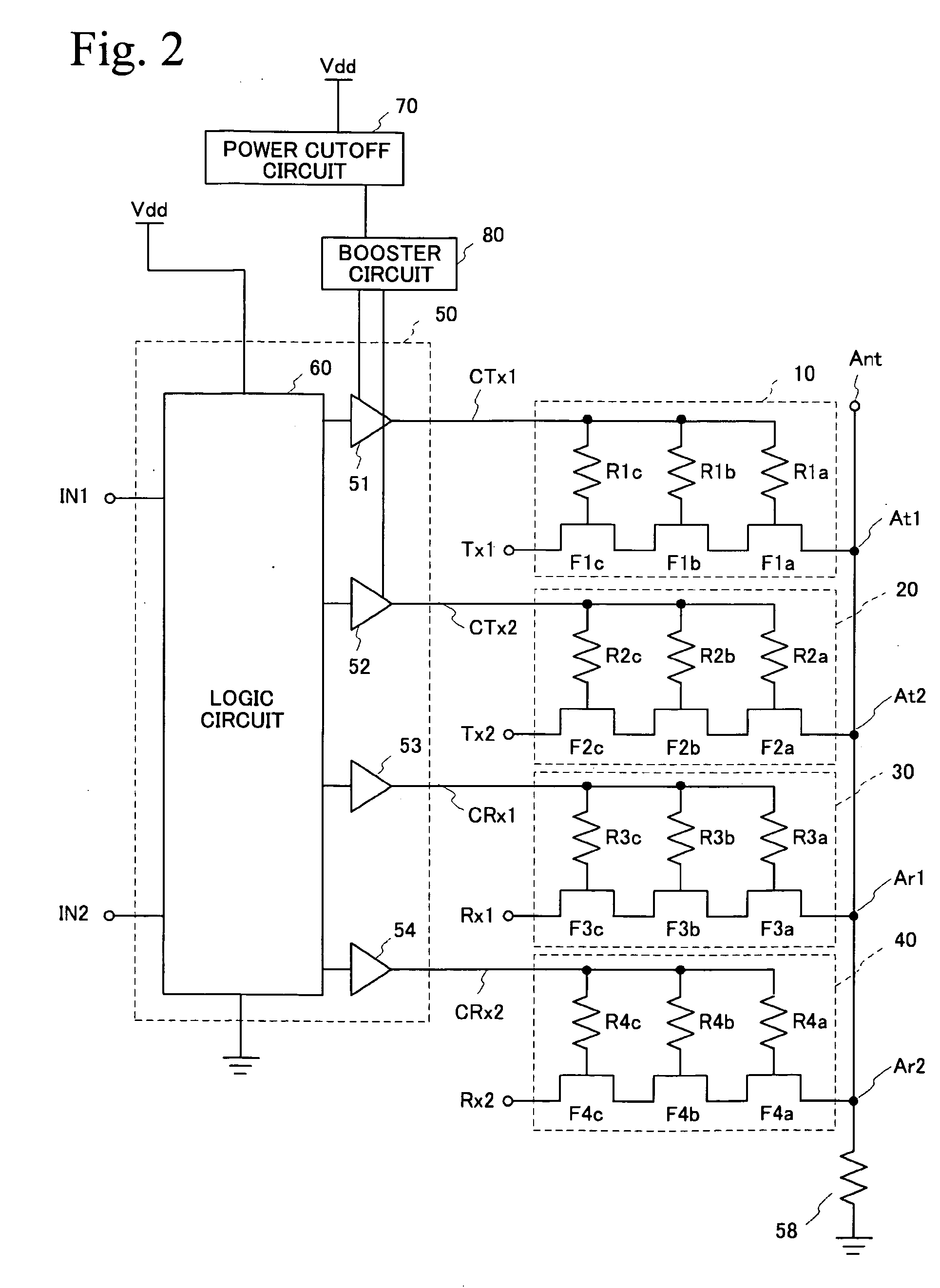
[0027] A first embodiment is an exemplary SP4T for use in portable telephones. FIG. 2 is a circuit diagram of a switch circuit in accordance with the first embodiment, and FIG. 3 is a circuit diagram of a control circuit 50 shown in FIG. 2. FIG. 4A is a circuit diagram of a booster circuit 80 and a power cutoff circuit 70 shown in FIG. 2, and FIG. 4B is a circuit diagram of drive circuits 51 and 52 shown therein. Referring to FIG. 2, the transmission switches 10 and 20 are connected to the antenna terminal Ant via the terminals At1 and At2, respectively, and the reception switches 30 and 40 are connected to the antenna terminal Ant via the terminals Ar1 and Ar2 (second terminals). A portion in which the antenna terminal Ant and the terminals At1, At2, Ar1 and Ar2 are connected is defined as common connection portion. The antenna terminal Ant is grounded via the bias resistor 58. The transmission switch 10 includes three FETs F1a through F1c and three resistors R1a through R1c, and t...
second embodiment
[0045] A second embodiment uses power leakage via the reception switch 40 instead of the oscillator 82 of the booster circuit 80 in the switch circuit of the first embodiment. FIG. 5 is a circuit diagram of a switch circuit in accordance with the second embodiment. Referring to FIG. 5, the second embodiment has the switches 10, 20, 30 and 40 and the control circuit 50 used in the first embodiment. Parts that are the same as those shown in the previously described figures are given the same reference numerals. A booster circuit 100 is connected to the output terminal Rx2 of the reception switch 40 via a signal cutoff circuit 90. The output Pump of the booster circuit 100 is connected to the drive circuits 51 and 52.
[0046] The signal cutoff circuit 90 has an FET F9 in which the source and drain are respectively connected to the output terminal Rx2 and the booster circuit 100, and the gate is connected to a node Cont2 via a resistor R9. The node Cont2 is connected to the logic circuit...
third embodiment
[0051] A third embodiment has a configuration in which a noise filter and a voltage clamp circuit are connected to the output of the booster circuit 80. FIG. 6 is a circuit diagram of the booster circuit 80 and its peripheral circuits in accordance with the third embodiment. The third embodiment employs the switches 10 through 40 and the control circuit 50 as in the case of the first embodiment although these elements are not illustrated in FIG. 6. The power cutoff circuit 70 and the booster circuit 80 are the same as those used in the first embodiment, and are assigned the same reference numerals. The output of the booster circuit 80 passes through a filter circuit 110, and is connected to the drive circuits 51 and 52 via the node Pump. The filter 110 is a high-pass filter composed of a capacitor C11 and an inductor L11, and functions to eliminate noise from the booster circuit 80. A voltage clamp circuit 120 is connected to the node Pump. The voltage clamp circuit 120 is made of d...
PUM
 Abstract
Description
Claims
Application Information
 - R&D
- Intellectual Property
- Life Sciences
- Materials
- Tech Scout
- Unparalleled Data Quality
- Higher Quality Content
- 60% Fewer Hallucinations
Browse by: Latest US Patents, China's latest patents, Technical Efficacy Thesaurus, Application Domain, Technology Topic, Popular Technical Reports.
© 2025 PatSnap. All rights reserved.Legal|Privacy policy|Modern Slavery Act Transparency Statement|Sitemap|About US| Contact US: help@patsnap.com