EUV exposure mask blanks and their fabrication process, and EUV exposure mask

Inactive Publication Date: 2007-01-18
DAI NIPPON PRINTING CO LTD
View PDF2 Cites 7 Cited by
  • Summary
  • Abstract
  • Description
  • Claims
  • Application Information

AI Technical Summary

Benefits of technology

[0012] In view of such problems as mentioned above, an object of the present invention is to provide a mask blank for EUV exposure wherein a substrate is provided at its flank with an electrically conductive film unlikely to peel off in EUV exposure mask fabrication process steps, etc. an

Problems solved by technology

With a mask attached to an aligner for implementing EUV exposure, as the mask sags even a bit due to its own weight, it brings on a misalignment in the post-transfer pattern.
However, the EUV exposure mask having an electrically conductive layer is often likely to remain clinging firmly to the electrostatic chuck after EUV exposure, rendering its removal hard; there are problems arising in connection with the time taken for detachment operat

Method used


Image

  • EUV exposure mask blanks and their fabrication process, and EUV exposure mask
  • EUV exposure mask blanks and their fabrication process, and EUV exposure mask
  • EUV exposure mask blanks and their fabrication process, and EUV exposure mask

Examples


first embodiment

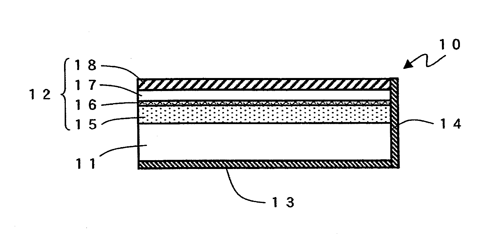
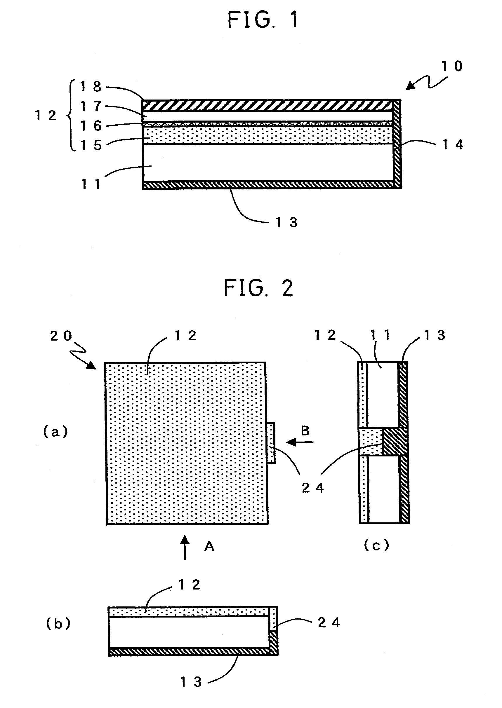
[0069] The first embodiment is directed to the EUV exposure mask blank fabrication process wherein a thin-film layer that forms a mask blank is formed by a vacuum film-formation technique using a mask holder having a cutout space at a site where a flank conductive film is to be formed and, at the same time, the flank conductive film is formed.

[0070] With the EUV exposure mask blank of FIG. 3 in mind, reference is made to FIG. 5.

[0071] The pattern-formation layer 12 is formed on one major surface of the substrate 11 at a given thickness as by sputtering, and then placed in a mask holder 51 having a cutout space 52, as depicted in FIG. 5(a). FIG. 5(b) is a sectional view as taken on A-A line in FIG. 5(a).

[0072] Then, as depicted in FIG. 5(c), the electrically conductive layer 13 is formed on another major surface of the substrate 11 at a given thickness as by sputtering. FIG. 5(d) is a sectional view as taken on B-B line in FIG. 5(c). Simultaneously with this, the flank conductive ...

second embodiment

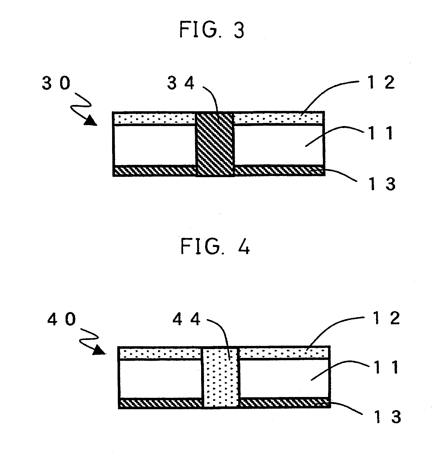
[0073] The second embodiment is directed to a process of fabricating an EUV exposure mask blank having a flank conductive film by a liftoff technique, which process is well fit for where, upon formation of films on both major surfaces of the substrate, the sputtered films do not fully come down to the flank.

[0074] As depicted in FIG. 6(a), the pattern-formation layer 12 is provided on one major surface of the substrate 11 at a given thickness as by sputtering, and the electrically conductive layer 13 is formed on another major surface of the substrate 11 at a given thickness as by sputtering.

[0075] Then, a liftoff material is coated or laminated on the conductive layer 13 to form a liftoff layer 65 of about 0.1 to 1 μm in thickness. For the liftoff layer 65, for instance, a layer obtained by coating of a photosensitive resin solution or a dry film is used.

[0076] Then, as depicted in FIG. 6(b), the above substrate is placed in a mask holder 61 having a cutout space 62.

[0077] Then...

third embodiment

[0079] The third embodiment is directed to a process of fabricating an EUV exposure mask blank having a flank conductive film by masking using a blocking plate, which process is well fit for where, upon formation of films on both major surfaces of the substrate, the sputtered films do not fully come down to the flank.

[0080] As depicted in FIG. 7(a), the pattern-formation layer 12 is provided on one major surface of the substrate 11 at a given thickness as by sputtering, and the electrically conductive layer 13 is formed on another major surface of the substrate 11 at a given thickness as by sputtering.

[0081] Then, as depicted in FIG. 7(b), the above substrate is placed in a mask holder 71 having a cutout space 72. Then, the flank of the substrate and the conductive layer 13 are covered up with a blocking plate 75 except the position to be provided with the desired conductive film.

[0082] Then, as depicted in FIG. 7(c), an electrically conductive material is sputtered or otherwise ...


PUM

PropertyMeasurementUnit
Electrical conductivityaaaaaaaaaa
Electrical conductoraaaaaaaaaa

Abstract

The invention provides a mask blank for EUV exposure wherein a substrate is provided at its flank with an electrically conductive film unlikely to peel off in EUV exposure mask fabrication process steps, etc. and its fabrication process, and provide a mask for EUV exposure which is readily attachable to or detachable from an electrostatic chuck, thereby foreclosing the possibility of the mask remaining clinging firmly to the electrostatic chuck after EUV exposure and being hard to detach from it. A mask blank for EUV exposure is provided, in which on one major surface of a substrate, a reflective layer adapted to reflect EUV light and an absorptive layer located on said reflective layer for absorption of said EUV light are at least provided as a pattern-formation layer. An electrically conductive layer is formed on another major surface of the substrate, and the pattern-formation layer and the conductive layer on the opposite major surfaces of the substrate are in conduction with each other via one or more flank conductive films provided at the flank of the substrate.

Description

BACKGROUND OF THE INVENTION [0001] The present invention relates generally to a mask blank for lithography in the fabrication of semiconductor devices, etc. and its fabrication process as well as a mask for lithography, and more particularly to a mask blank for EUV exposure (EUV is an acronym of extreme ultraviolet) for the fabrication of the mask to transfer a mask pattern onto a wafer using EUV and its fabrication process as well as a mask for EUV exposure. [0002] As semiconductor devices are now much finer, there is an exposure technique available, in which patterns are transferred onto wafers under photomasks, employing optical projection aligners using KrF or ArF excimer lasers. Before long, however, exposure techniques relying on such optical projection aligners would reach their own resolution limits; so there are new transfer techniques proposed such as direct lithography by electron beam lithography systems, electron beam projection lithography: EPL), low energy electron be...

Claims


Application Information

Patent Timeline
IPC IPC(8): G03F1/00C23C14/04G03F1/24G03F1/40H01L21/027
CPCB82Y10/00B82Y40/00G03F1/38G03F1/24G03F1/14G03F1/62
Inventor ABE, TSUKASASASAKI, SHIHO
Owner DAI NIPPON PRINTING CO LTD
Why Eureka
Try Eureka