Nanotube probe and method for manufacturing the same

a nanotube and probe technology, applied in the field of nanotube probes, can solve the problems of difficult even to fix the nanotube, difficult to observe directly a nanotube as small as 100 nm, and requires a very high level of microscopic processing technology, and achieves the effects of high accuracy, short time, and easy formation

Inactive Publication Date: 2007-01-25
NAKAYAMA YOSHIKAZU +1
View PDF3 Cites 10 Cited by
  • Summary
  • Abstract
  • Description
  • Claims
  • Application Information

AI Technical Summary

Benefits of technology

[0032] According to the first embodiment of the present invention, as the nanotube is fastened to the holder by means of partial coating films, drastic reduction of time required for forming the coating film, compared to the conventional overall coating film, is made possible by making the size of the partial coating film as small as possible. A nanotube is generally hard to be visualized in entirety even under such a magnifying device as electron microscope. In particular, it is difficult even for a skilled observer to identify the end of a nanotube. Since the overall coating method requires that the furthest back end of the nanotube is visually identified in the process of coating, it involves enormous length of time for coating. On the other hand, in the case of partial coating film method, this requirement for identifying the back end of the nanotube is completely eliminated, whereby such advantages as shortened time of coating film formation and extremely simplified coating operation can be accomplished. In other words, because the operation is nothing more than applying partial coating at two positions, at the least, identified under microscope, practicability of the manufacturing operation can be improved drastically. Furthermore, although fastening the nanotube at minimum two positions on the base end portion of the nanotube is sufficient to keep the nanotube fixed, it is possible to increase the fastening points to three or four points.
[0046] According to the fifteenth embodiment of the present invention, the size of the coating, i.e. the coating length L, the maximum coating skirt width W can be freely changed by regulating the scanning range (beam oscillation width) of the electron beam or ion beam. Thus, said conditions, W / d≧0.1 and L / d≧0.3, can be easily satisfied. Furthermore, as it is possible to minimize the beam diameter of the electron beam or the ion beam, it can effectively minimize deposition of decomposed substances on other area than the coating area. In addition, since the average coating film thickness can be controlled by regulating the beam irradiation time, said condition of film thickness, i.e. T≧1 (nm) can be easily achieved.

Problems solved by technology

However, fastening of the nanotube on a holder to retain the needle probe has required very high level of microscopic processing technology.
However, as the maximum magnification of an optical microscope is limited to 1000 to 2000 times, it was difficult, in principle, to observe directly a nanotube which is as small as 100 nm or less.
Thus, it was difficult even to fix the nanotube to a certain location on the protruded portion of a cantilever, and it was still harder to control the number of fixed nanotubes as well as the orientation thereof.
To make the matter worse, it often happened that more than one nanotube were fastened, causing the obtained image to become overlapped or that the angle of the probe needle set with reference to the observed surface deviated far from 90° causing erroneous image to be generated.
As the result, some of said nanotube probes were too much stained with the impurities to be offered as a commodity.
Such displaced fastening of nanotube can lead to a problem that the sharp end of the protruded portion 107 may function as a probe needle as well as the end of the nanotube 108C in an AFM measurement.

Method used


Image

  • Nanotube probe and method for manufacturing the same
  • Nanotube probe and method for manufacturing the same
  • Nanotube probe and method for manufacturing the same

Examples


Embodiment Construction

[0064] The inventor of the present invention and his team have made strenuous development efforts to improve the nanotube probe constructed by the overall coating method, with a result that a nanotube probe by way of partial coating films have been completed. Following are more detailed description of the present invention related to nanotube probes and manufacturing method thereof with reference to the accompanying drawings.

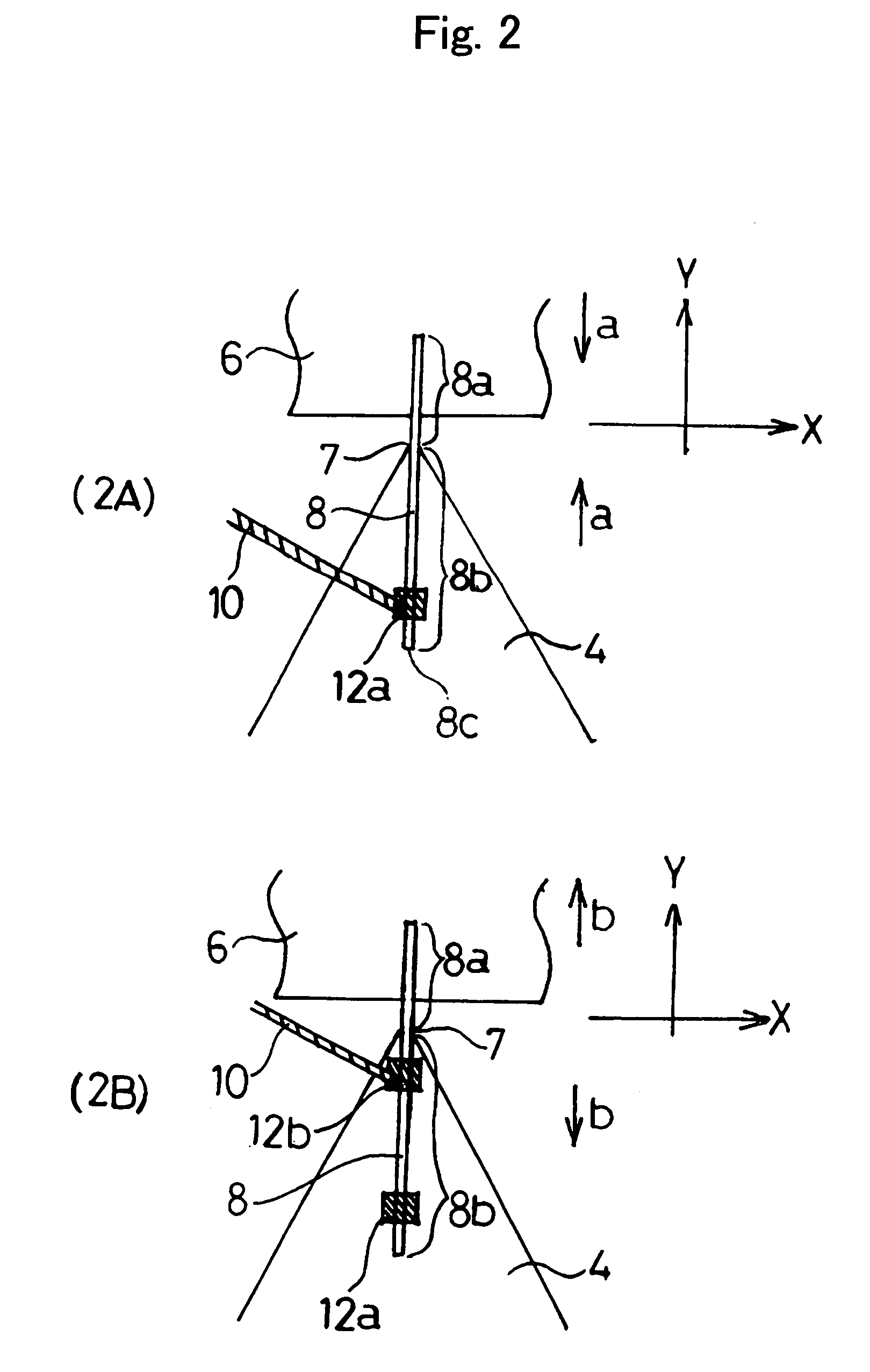
[0065] This partial coating method provides for a nanotube probe and manufacturing method thereof, wherein a nanotube can be fastened to a surface of a holder in short time, the amount of impurities adhering to the holder surface can be reduced to a bare minimum, and an arbitrary shape of holder can be used.

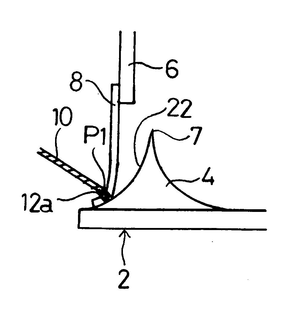
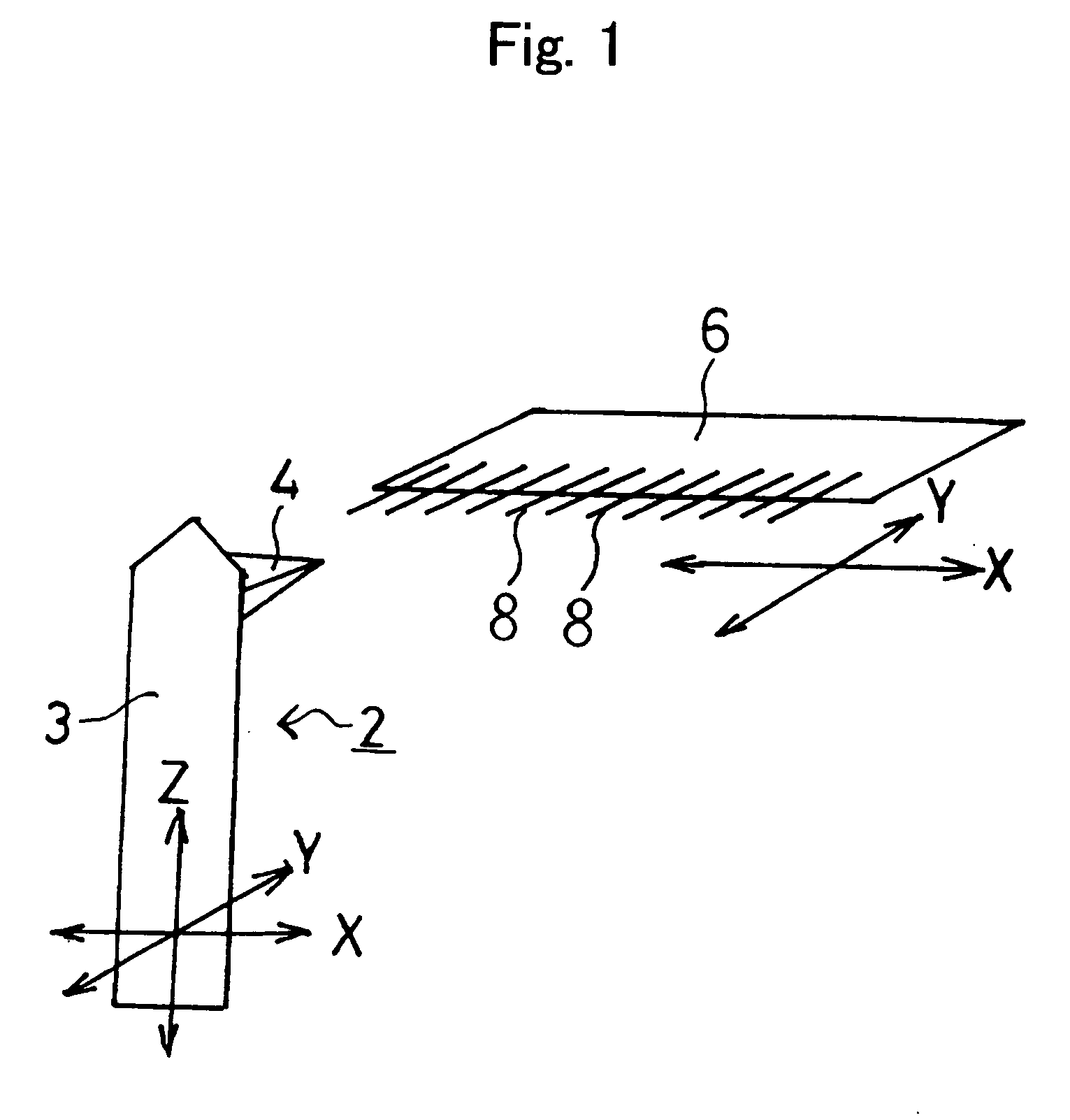
[0066] In the following description of embodiments, a protruded portion of a cantilever used for AFM is used as a holder on which a nanotube is fastened. However, the holder is not limited to cantilevers, but any other component on which a nanotube can be f...


PUM

PropertyMeasurementUnit
thicknessaaaaaaaaaa
angleaaaaaaaaaa
diameteraaaaaaaaaa

Abstract

The present invention realizes a nanotube probe with high durability that can be manufactured in short time with less impurities adhered to the holder sustaining the nanotube. The nanotube probe according to this invention is constructed by fastening a nanotube 8 on the protruded portion 4 of a cantilever by way of at least two partial coating films 12a and 12b. One or more additional partial coating films may be formed in the intermediate area between these two partial coating films. Each partial coating film is formed by irradiating electron beam 10 on the position where the nanotube 8 is in contact with the protruded portion 4 of the cantilever. The partial coating films are separated not to overlap each other. By minimizing the size of partial coating film as well as by narrowing down the beam diameter, coating time may be further shortened. With the beam diameter narrowed down, excessive deposit of impurities can be put under control.

Description

TECHNICAL FIELD [0001] The present invention relates to a nanotube probe utilizing nanotube as a probe needle. More particularly, the present invention relates to a nanotube probe which realizes a concrete method for fastening a nanotube to a holder, and which can be used, for instance, as a probe needle in a scanning probe microscope that picks up images of surface of samples by detecting physical or chemical actions on the sample surfaces, and it further relates to a method of manufacturing such a nanotube probe. BACKGROUND ART [0002] A scanning probe microscope is a microscope in which a probe needle detects physical or chemical actions from surface atoms of a sample while it is scanned across the surface so that the image of sample surface can be generated from the detected signals. Consequently, the resolving power and measurement accuracy of the scanning probe microscope depend to a large extent on the size and physical properties of the probe needle. [0003] The use of a nanot...

Claims


Application Information

Patent Timeline
Patent Type & Authority Applications(United States)
IPC IPC(8): G21K7/00G01Q60/16G01Q60/38G01Q70/00G01Q70/02G01Q70/12
CPCB82Y15/00G01Q70/12B82Y35/00G01Q70/16
Inventor NAKAYAMA, YOSHIKAZUOKAWA, TAKASHIYAMANAKA, SHIGENOBUHARADA, AKIO
Owner NAKAYAMA YOSHIKAZU
Why Eureka
Try Eureka