

Method for arraying nano material and method for fabricating liquid crystal display device using the same
a liquid crystal display device and arraying technology, applied in semiconductor devices, instruments, electrical devices, etc., can solve the problems of increasing manufacturing costs, affecting the formation of inorganic semiconductor layers, and causing a lot of problems
- Summary
- Abstract
- Description
- Claims
- Application Information
AI Technical Summary
Benefits of technology
Problems solved by technology
Method used
Image

Examples
first embodiment
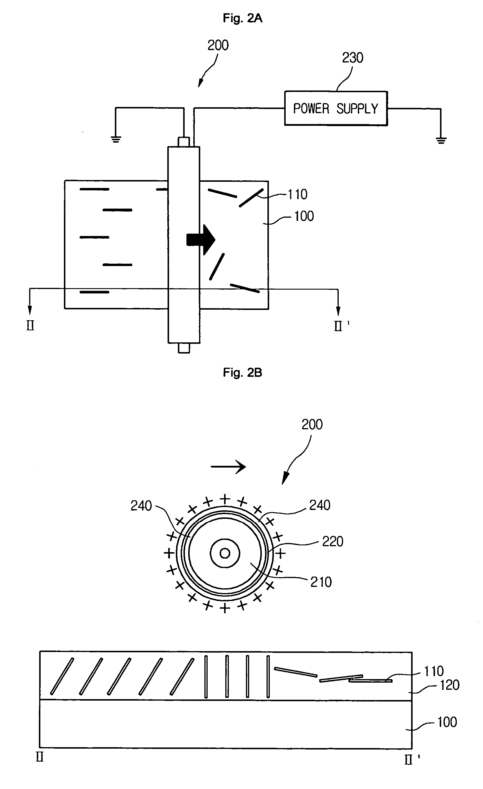
[0029]FIGS. 2A and 2B are views for explaining an apparatus and method for arraying nano material according to the present invention. Specifically, FIG. 2A is a plan view illustrating a process of arraying nano material and FIGS. 2B and 2C are sectional views taken along line II-II′ of FIG. 2A.
[0030] Referring to FIGS. 2A to 2C, a dispersion solution 120 where nano materials 100 are dispersed is coated on a substrate 100 by a typical method. Examples of the typical method include an inkjet printing, a spin coating, a deep coating, and a doctor blade. However, the present invention is not limited to these methods.
[0031] The nano materials 110 dispersed in the dispersion solution 120 are arrayed in a random direction. The nano materials 110 may be nanowires or nanotubes. Also, the nano materials 110 can be a dielectric material and, more particularly, may be at least one material selected from the group consisting of Si, Ge, Sn, Se, Te, B, C, P, GaN, ZnO, SiO2, and Al2O3.
[0032] Also...
PUM
 Abstract
Description
Claims
Application Information