Error correcting memory access means and method

a memory access and error correction technology, applied in the field of memory devices, can solve the problems of high cost per unit attributable to testing, and high cost per unit of testing, so as to reduce the cost of device testing and thereby the cost of the device itself, and efficiently utilize error correction. , the effect of reducing the cost of testing costs

Active Publication Date: 2007-02-01
WESTERN DIGITAL TECH INC
View PDF3 Cites 21 Cited by
  • Summary
  • Abstract
  • Description
  • Claims
  • Application Information

AI Technical Summary

Benefits of technology

[0010] The present invention is a means and a method for addressing streams of data stored within a memory device so as to minimize the cost of device testing and thereby the cost of the device itself. Solid-state memory is typically thought of as working in random access mode. As such, most solid-state memory is designed for error-free operation. However, many emerging applications require data that is accessed in long blocks. For such applications, these blocks can efficiently utilize error correcting. The present invention is a means and a method for accessing the locations in a memory device so as to avoid having error correcting techniques fail due to such common memory device faults as shorts or breaks among the row lines and column lines or as defective data bit storage elements. By enabling error correcting memory to function even when such common flaws exist, testing costs can be significantly reduced while maintaining high device yields. Finally, this addressing approach is applied in the same way regardless of whether the data is being written into or read out of the device.
[0011] By reducing the cost of solid state memory through the reduction of the testing costs, the present invention can also be used to reduce the cost of systems which use large amounts of data. As is the case with CD-ROM and DVD systems, this error corrected, solid-state data storage in these systems can be fixed or removable and interchangable or a combination of the two. These systems can range from computers to personal digital assistants (PDA's) to digital cameras.

Problems solved by technology

Current memory testing costs are significant and are expected to grow as the capacity of the devices grows.
As a result, the cost per unit attributable to testing should rise.
However, this requires that each device be thoroughly tested in order to identify the locations of the faults and this extensive testing can be very expensive, especially when the number of bytes of memory is very large.
The subsequent post-manufacturing error correcting of this approach further increases the cost of the device.
Typically, as the size of a block of data increases, the number of error correcting bits increases more slowly; this results in a smaller percentage of error correcting bits as the size of the data block grows.
While it is possible that any given bit in the array is flawed and inoperative, one must also worry about other failure modes.
One common failure mode occurs when one of these rows or columns has a break in it thereby making a portion of the array addressed by that row or column inaccessable.
Alternatively, another common failure mode occurs when a short circuit exists between adjacent rows, adjacent columns, or a row and a column thereby making it impossible to separately address bits accessed by the shorted together rows or columns.
Therefore, as with the application of error correcting for CD-ROM and DVD, too many bits may be lost in a given block of bits for the error correcting algorithm and error correcting bits to be able to correct for these errors.
Presently, in some applications such as digital photography and music and video playback, to name a few, memory is so expensive that its cost often greatly exceeds the value of the data contained within it.
However, CD-ROM and DVD are inconvenient because they are fragile and consume large amounts of power due to their lasers, motors and servo mechanisms.

Method used


Image

  • Error correcting memory access means and method
  • Error correcting memory access means and method
  • Error correcting memory access means and method

Examples


Embodiment Construction

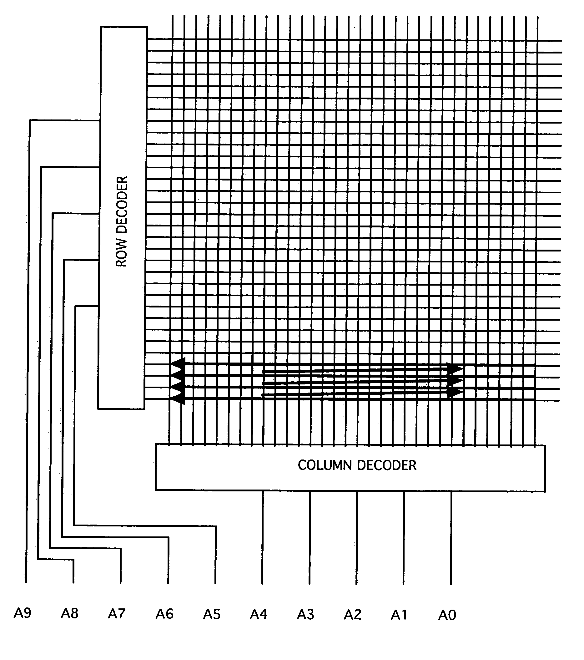
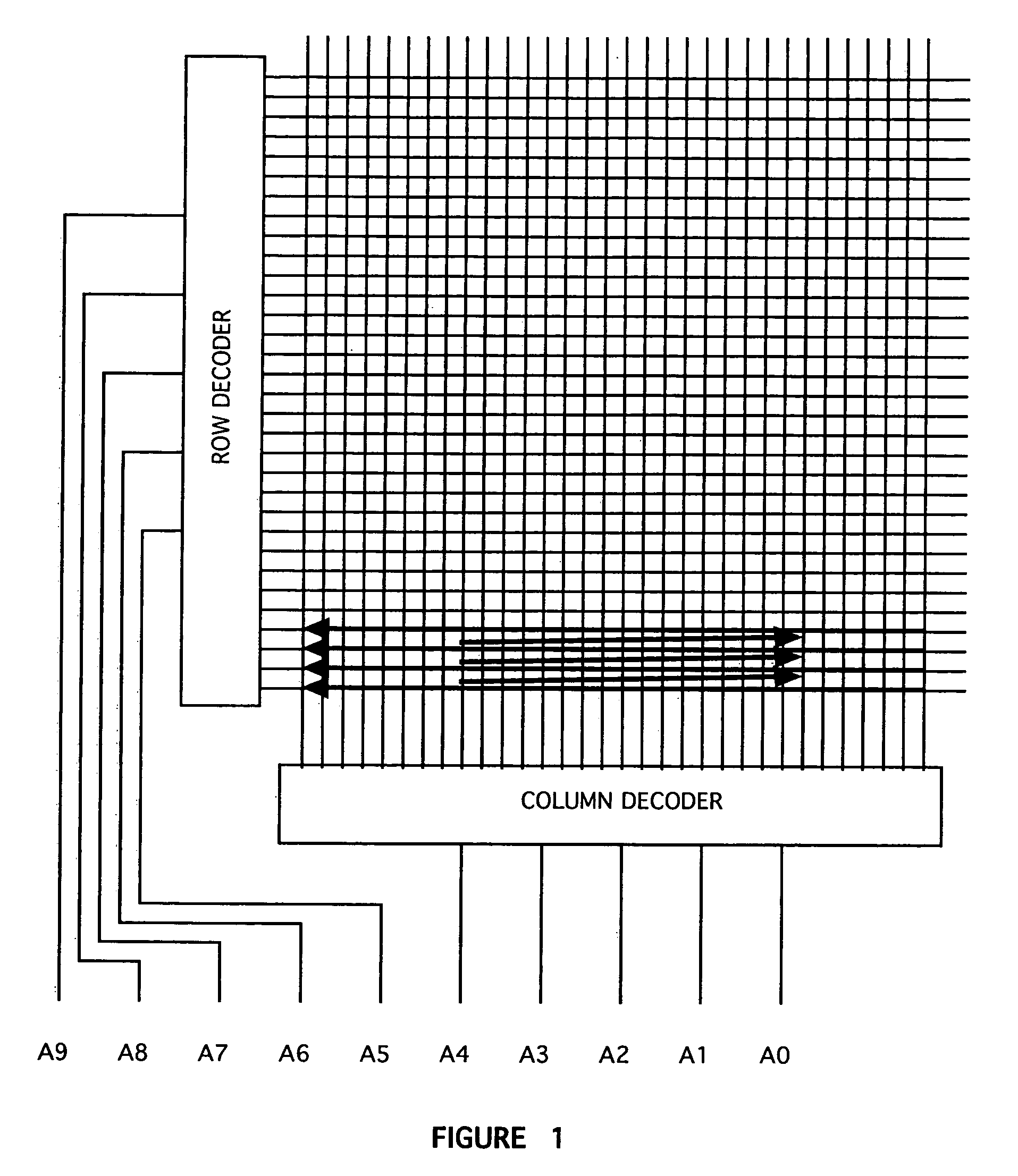
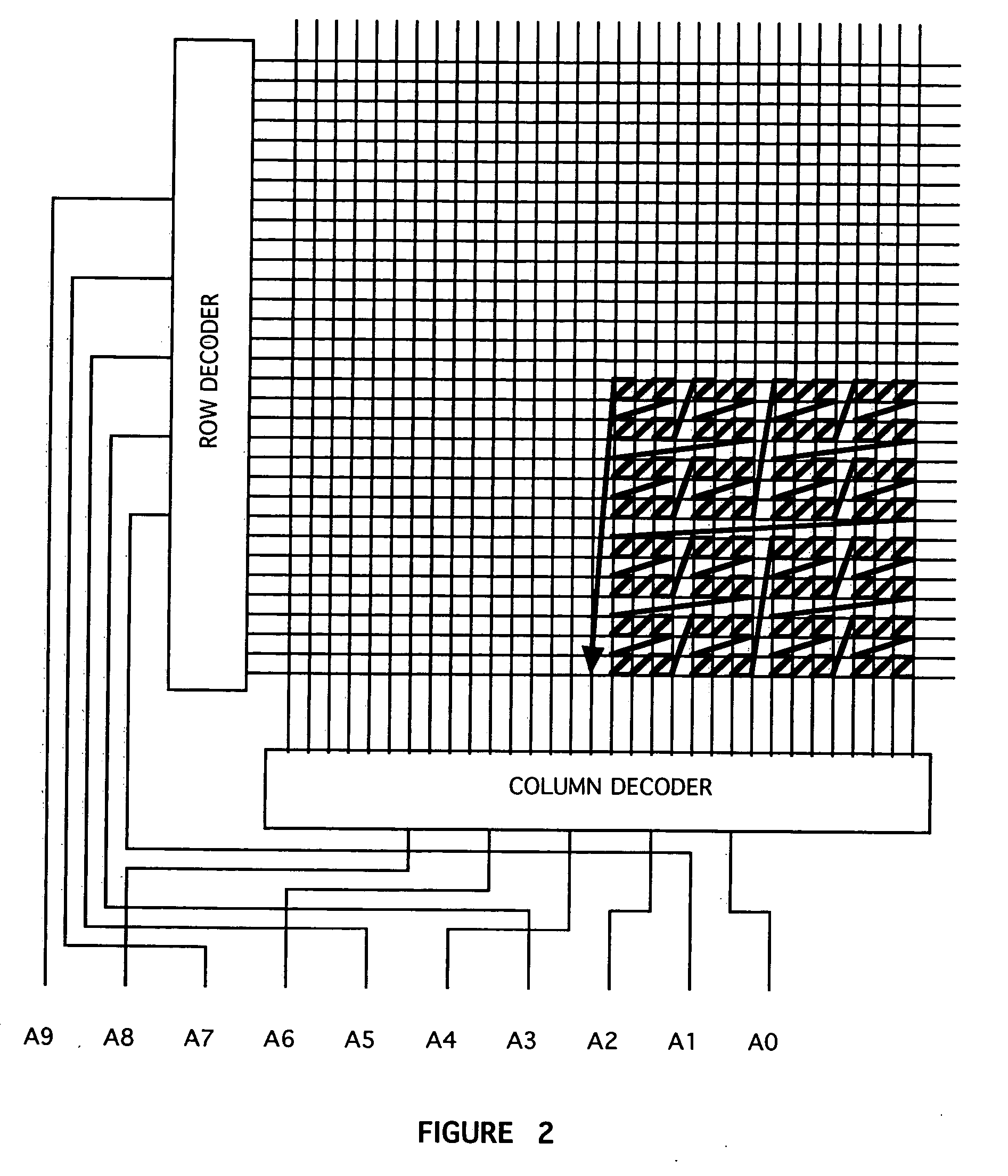
[0015] The present invention is a means for accessing memory in a way that better facilitates error correcting within the memory device. In non-electronic storage devices such as CD-ROM and DVD, data is accessed in sectors or blocks. That is to say that the data is accessed not bit by bit or byte by byte, but rather as a block of data from which individual bits or bytes can then be read (when writing, the data bits or bytes are written to the data block which is then enhanced with error-correcting bits and the block is copied to the memory device). Included within this block of data are error-correcting bits which through an algorithm (e.g., hamming codes and other error correcting techniques as are well known to those skilled in the art) can detect the presence of erroneous data bits and can correct those error bits (up to a maximum number of correctable error bits per block as determined by the number of error correcting bits and the error correcting algorithm employed). By doing ...


PUM


Abstract

As advances continue to be made in the area of semiconductor memory devices, high capacity and low cost will be increasingly important. In particular, it will be necessary to create memory devices for which the testing of the device must be minimized in order to minimize costs. Current memory manufacturing costs are significant and will grow as the capacity of the devices grows—the higher the memory's capacity, the more storage locations that must be tested, and the longer the testing operation will take. The cost of the testing can be calculated by dividing the amortized cost of the test equipment by the number of devices tested. As memory devices enter the Gigabyte range and larger, the number of devices that can be tested by a given piece of test equipment will go down. As a result, the cost per unit attributable to testing will rise. The present invention is a means and a method for accessing streams of data stored within a memory device so as to minimize the cost of device testing and thereby the cost of the device itself. By incorporating error-correcting bits in the data stream, the individual data bits need not be tested. Then, by accessing the memory locations so as to avoid having error correcting techniques fail due to common memory device faults, testing costs can be significantly reduced while maintaining high device yields. A sequential access of the memory device will access data bits in a somewhat diagonal path across the two-dimensional array. The key to the present invention is that the sequential data stream stored in the device is stored such that sequential access of that data will not dwell on a single (or a small number of) row or column line. In a three or more dimensional array, the sequential data stream stored in the device is stored such that sequential access of that data will not dwell on a single value in a given dimension for which bulk errors are considered likely.

Description

CROSS-REFERENCE TO RELATED APPLICATIONS [0001] This application claims the benefits of U.S. Provisional Application No. 60 / 371,876, filed on Apr. 11, 2002, the entire disclosure of which is hereby incorporated by reference.FIELD OF THE INVENTION [0002] The present invention relates to memory devices which utilize error correcting, and more particularly to semiconductor memory devices in which the addressing pattern is optimized to better facilitate error correcting techniques and reduce device testing. BACKGROUND OF THE INVENTION [0003] As advances continue to be made in the area of semiconductor memory devices, high capacity and low cost will be increasingly important. In particular, it will be necessary to create memory devices for which the testing of the device must be minimized in order to minimize costs. Current memory testing costs are significant and are expected to grow as the capacity of the devices grows. The cost of the testing can be estimated by dividing the annual amo...

Claims


Application Information

Patent Timeline
Patent Type & Authority Applications(United States)
IPC IPC(8): G06F11/00G06F11/10G11C29/42H03M13/00
CPCG06F11/1008G11C2029/0409G11C29/42
Inventor SHEPARD, DANIEL ROBERT
Owner WESTERN DIGITAL TECH INC
Why Eureka
Try Eureka