
LED having improved soldering structure, method for soldering the LED to PCB, and LED assembly manufactured by the method

a technology of led and soldering structure, which is applied in the direction of sustainable manufacturing/processing, printed circuit aspects, and final product manufacturing, etc., can solve the problems of low moldability, difficult mounting side view, and difficulty in mounting, so as to improve the soldering structure and improve the soldering conditions. , the effect of saving the amount of solder pas

Inactive Publication Date: 2007-02-08
SAMSUNG ELECTRO MECHANICS CO LTD
View PDF3 Cites 12 Cited by
  • Summary
  • Abstract
  • Description
  • Claims
  • Application Information

AI Technical Summary

Benefits of technology

[0018] The present invention has been made to solve the foregoing problems of the prior art and therefore an object of certain embodiments of the present invention is to provide an LED having an improved soldering structure in which a hole / cutout part is formed in an external terminal portion of a lead for soldering, thereby improving soldering conditions while saving the amount of solder paste, a method of assembling the LED to a printed circuit board (PCB) via soldering, and an LED assembly manufactured by the assembling method.
[0019] Another object of certain embodiments of the invention is to provide an LED having an improved soldering structure in which a hole / cutout part for soldering is formed in an external terminal portion of a lead to increase bonding strength after the soldering, a method of assembling the LED to a printed circuit board (PCB), and an LED assembly manufactured by the assembling method.

Problems solved by technology

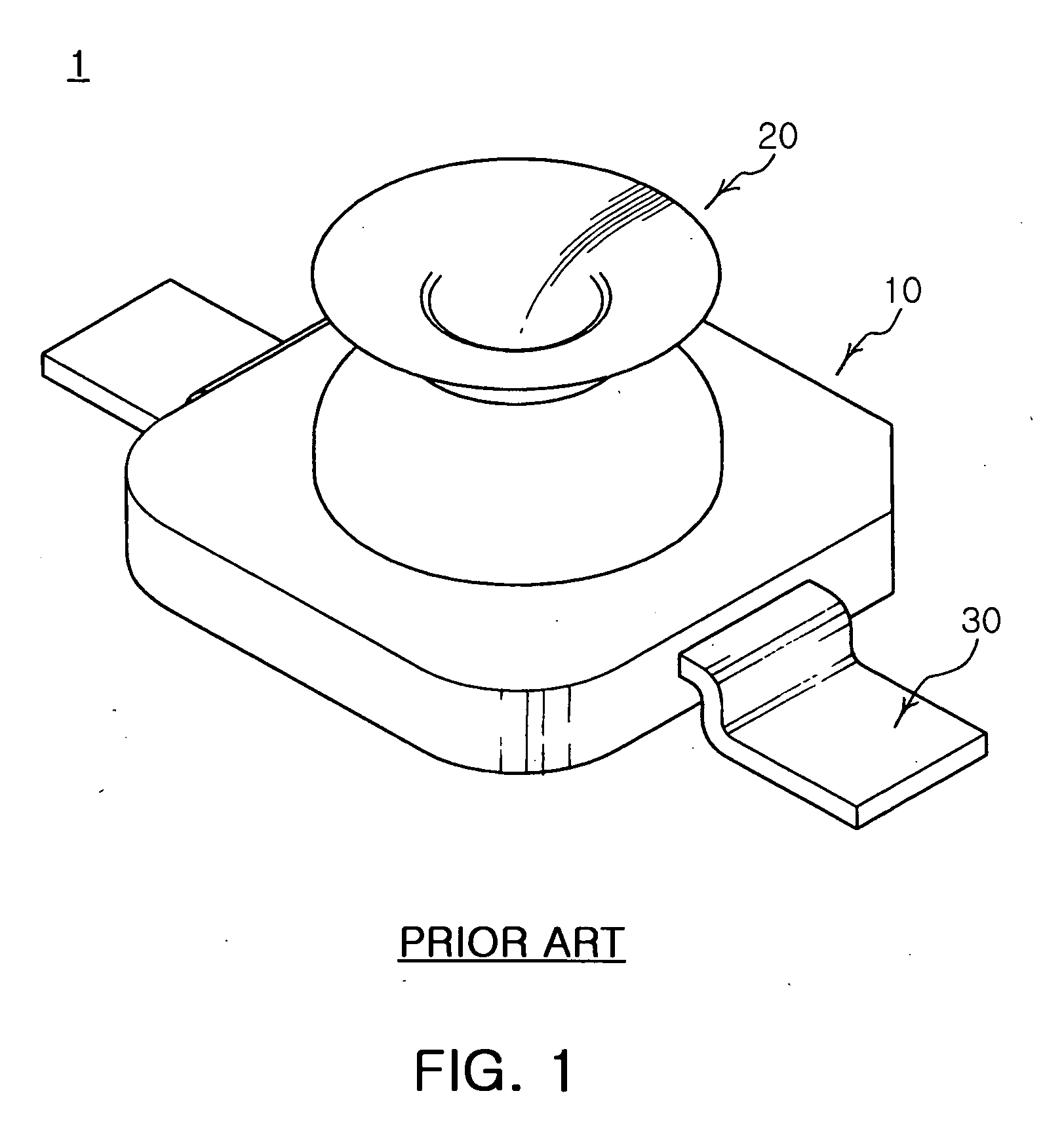
This is because a material that is resistant to heat has low moldability, and thus is not desirable for precisely forming the complex shape of the lens 20.
Therefore, it is difficult to mount the side view LED 1 shown in FIG. 1 in a high-temperature condition such as in the reflow process.
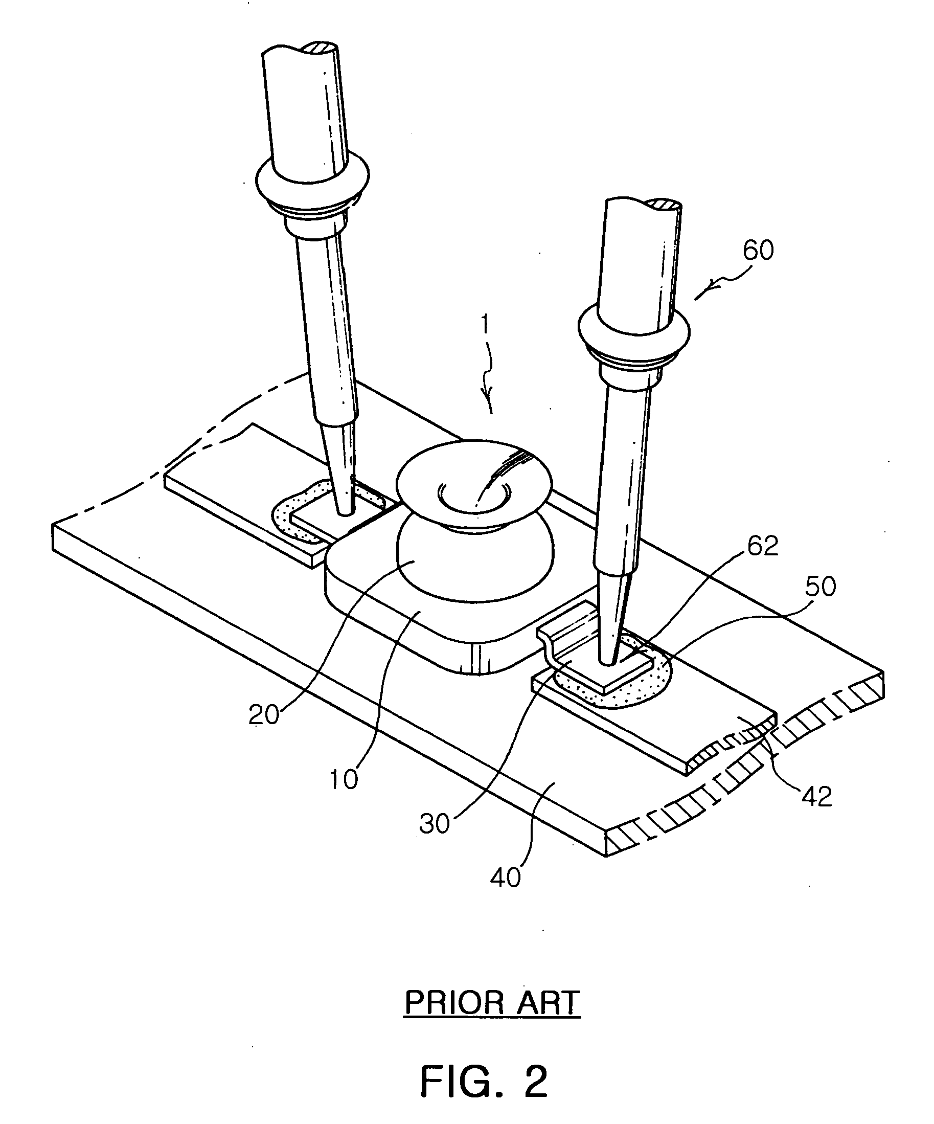
However, the conventional LED 1 and soldering procedures using the same have following problems.

Method used


Image

  • LED having improved soldering structure, method for soldering the LED to PCB, and LED assembly manufactured by the method
  • LED having improved soldering structure, method for soldering the LED to PCB, and LED assembly manufactured by the method
  • LED having improved soldering structure, method for soldering the LED to PCB, and LED assembly manufactured by the method

Examples


Embodiment Construction

[0048] Preferred embodiments of the present invention will now be described in detail with reference to the accompanying drawings.

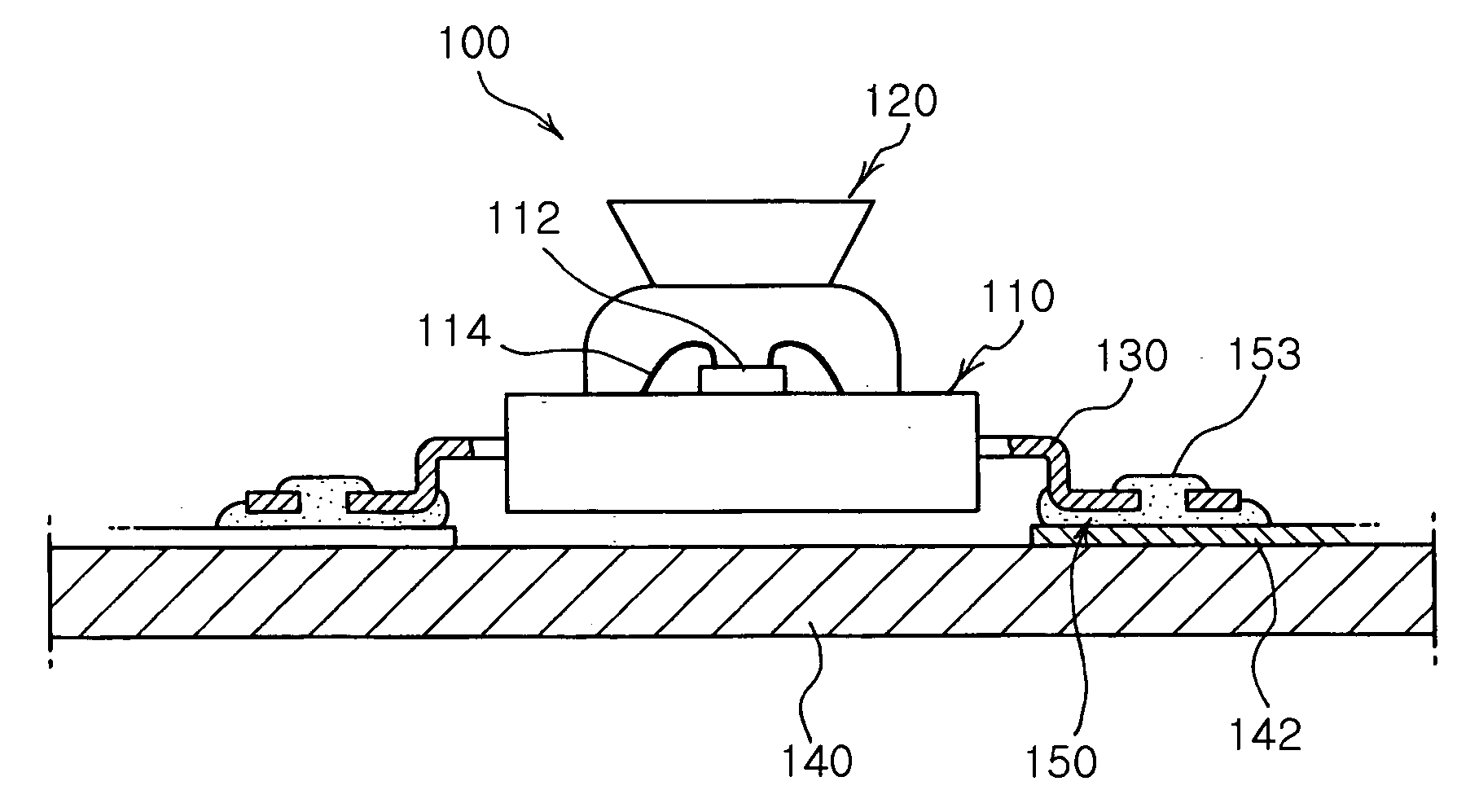
[0049] Referring to FIG. 5, a side view LED 100 according to the present invention includes a package body 110 with an LED chip 112 (see FIG. 11) mounted therein, a pair of leads 130 partially housed in the package body 110 and electrically connected to the LED chip to supply an external power and a transparent cover or lens 120 placed on an upper part of the package body 110 to protect the LED chip from an external environment and to laterally emit the light from the LED chip. In addition, an external terminal portion of the lead 130 has a hole 132 perforated therein.

[0050] Now, mounting procedures for mounting the LED 100 according to the present invention to a printed circuit board 140 such as a metal printed circuit board will be explained with reference to FIGS. 6 to 11.

[0051] First, as shown in FIGS. 6 to 8, a predetermined amount of solder paste...


PUM


Abstract

The invention relates to an LED with an improved soldering structure, a method of assembling the LED to a PCB, and an LED assembly manufactured by the method. The LED includes an LED chip and a pair of leads with an end electrically connected the LED chip and the other end to be connected to an external power source, having a hole or a cutout part formed therein. The LED also includes a package body housing a part of the lead in the side of the LED chip, and a transparent lens placed on a surface of the package body in the side of the LED chip, for emitting light laterally. This improves soldering conditions for soldering with the other end of the lead placed on the solder, saving the amount of a solder paste while enhancing bonding strength after soldering.

Description

CLAIM OF PRIORITY [0001] This application claims the benefit of Korean Patent Application No. 2005-70805 filed on Aug. 2, 2005, in the Korean Intellectual Property Office, the disclosure of which is incorporated herein by reference. BACKGROUND OF THE INVENTION [0002] 1. Field of the Invention [0003] The present invention relates to a light emitting diode (LED), and more particularly, to an LED having an improved soldering structure in which a hole / cutout part is formed in an external terminal portion of a lead to improve soldering conditions, thereby saving the amount of solder paste used and enhancing the bonding strength after soldering, to a method of assembling the LED to a printed circuit board (PCB) via soldering, and to an LED assembly manufactured by the assembling method. [0004] 2. Description of the Related Art [0005] In general, a light emitting diode (LED) is a semiconductor device for generating various colors of light when current is applied. The color of light generat...

Claims


Application Information

Patent Timeline
Patent Type & Authority Applications(United States)
IPC IPC(8): H01L33/00H01L21/00H01L33/54H01L33/56H01L33/62
CPCH01L33/486H01L33/62H05K3/3426H05K3/3494H05K2201/10106H05K2201/10651H01L2224/48091H05K2201/1084H05K2203/0195H01L2924/00012Y02P70/50H01L2924/00014
Inventor HAN, KYUNGLEE, SEONHAHM, HUNHAN, SEONGSONG, CHANGPARK, YOUNG
Owner SAMSUNG ELECTRO MECHANICS CO LTD
Learn More