Integrated circuit with low-stress under-bump metallurgy

a technology of integrated circuits and under-bump metallurgy, which is applied in the direction of semiconductor devices, semiconductor/solid-state device details, electrical apparatuses, etc., can solve the problems of affecting the copper consumption rate and subsequent intermetallic compound formation, the delamination of the solder ball, and the explosion of the on-chip routing

Inactive Publication Date: 2007-02-08
DELPHI TECH INC
View PDF3 Cites 25 Cited by
  • Summary
  • Abstract
  • Description
  • Claims
  • Application Information

AI Technical Summary

Problems solved by technology

Unfortunately, the high tin (Sn) content of lead-free solders has resulted in rapid consumption of copper from conventional UBMs, which has lead to solder ball delamination.
Unfortunately, the reliability of the bond formed between the solder ball and the copper layer depends upon the thickness of the copper layer, the solder type and the electrical and thermal exposure the bond experiences, which also affects the copper consumption rate and subsequent intermetallic compound formation.
In general, the increasing complexity of IC packing density has placed greater demand on the current carrying capability of flip-chip joints and has caused an explosion in on-chip routing.
However, complex on-chip routing tends to overwhelm the advantages gained by scaling transistors, due to transmission delays in signals passing between active devices.
These transmission delays are primarily due to a resistance-capacitance (RC) time constants of electrical interconnects.
Unfortunately, low-K dielectrics are notoriously fragile and do not have the necessary mechanical strength for many applications.
For example, commercially available low-K dielectrics have not been suitable in high-current flip-chip applications where copper bumps, e.g., mini-bumps or pillar-bumps, are utilized, due to the fact that the copper bumps result in relatively high-stresses derived from the substantial thickness, typically 80,000 angstroms or greater, of the copper bumps.
While copper mini-bumps can be formed in a non-equilibrium configuration that generates little stress in the IC substrate, a single heating cycle, such as the heating cycle that is required for solder reflow during assembly, may cause recrystallization of the copper grains and concurrent increases in film and IC substrate stress.

Method used


Image

  • Integrated circuit with low-stress under-bump metallurgy
  • Integrated circuit with low-stress under-bump metallurgy
  • Integrated circuit with low-stress under-bump metallurgy

Examples


Embodiment Construction

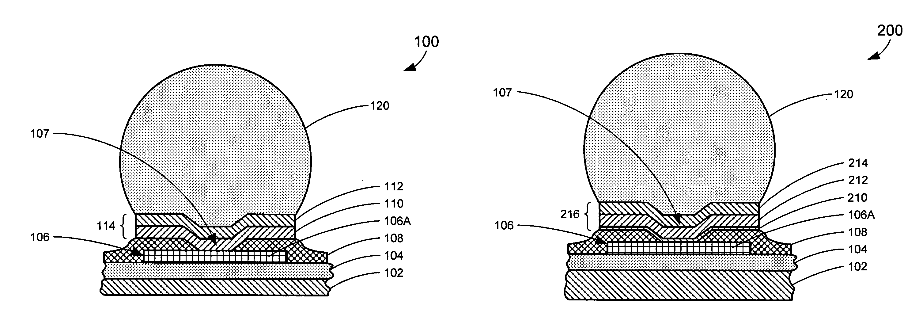
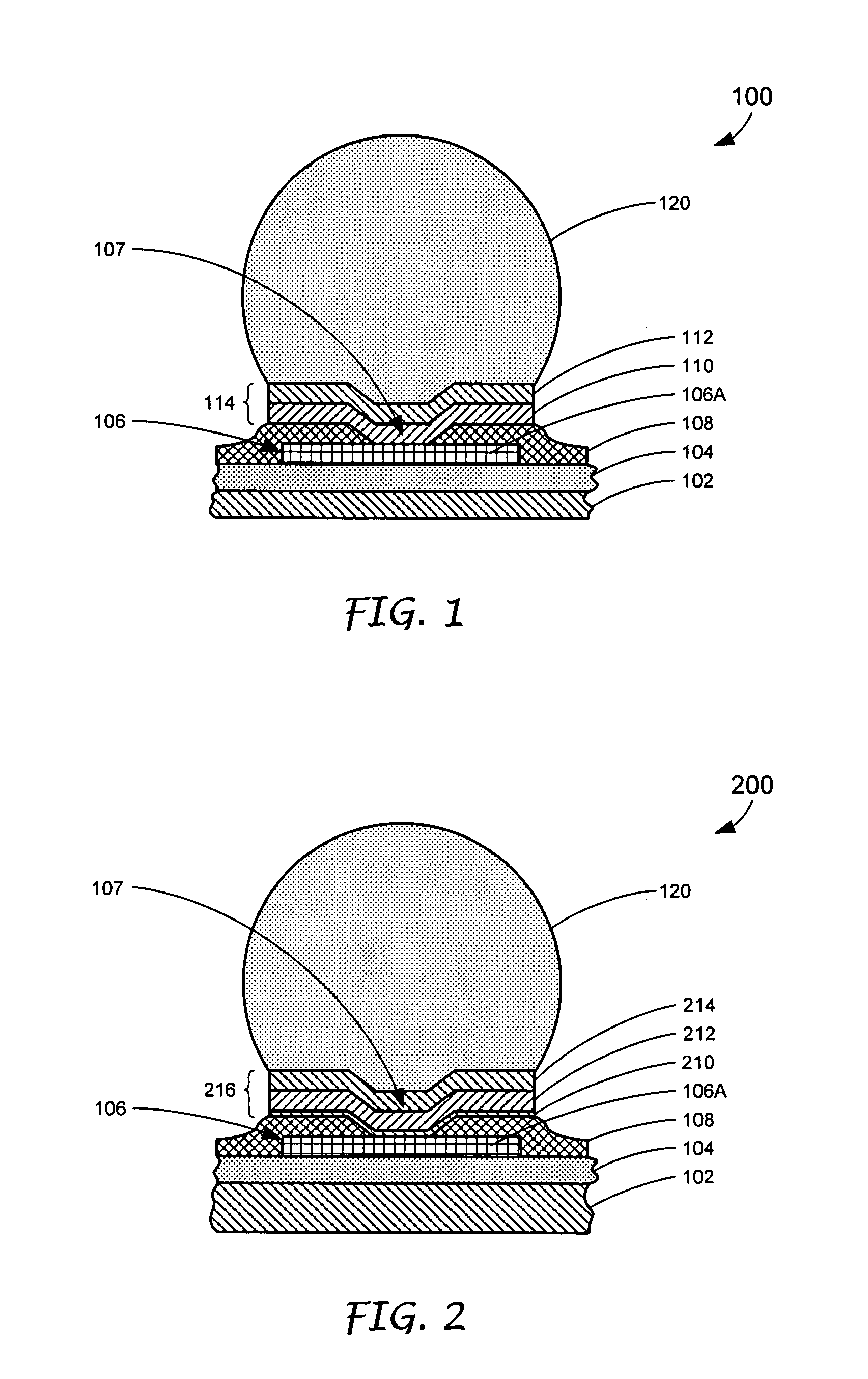
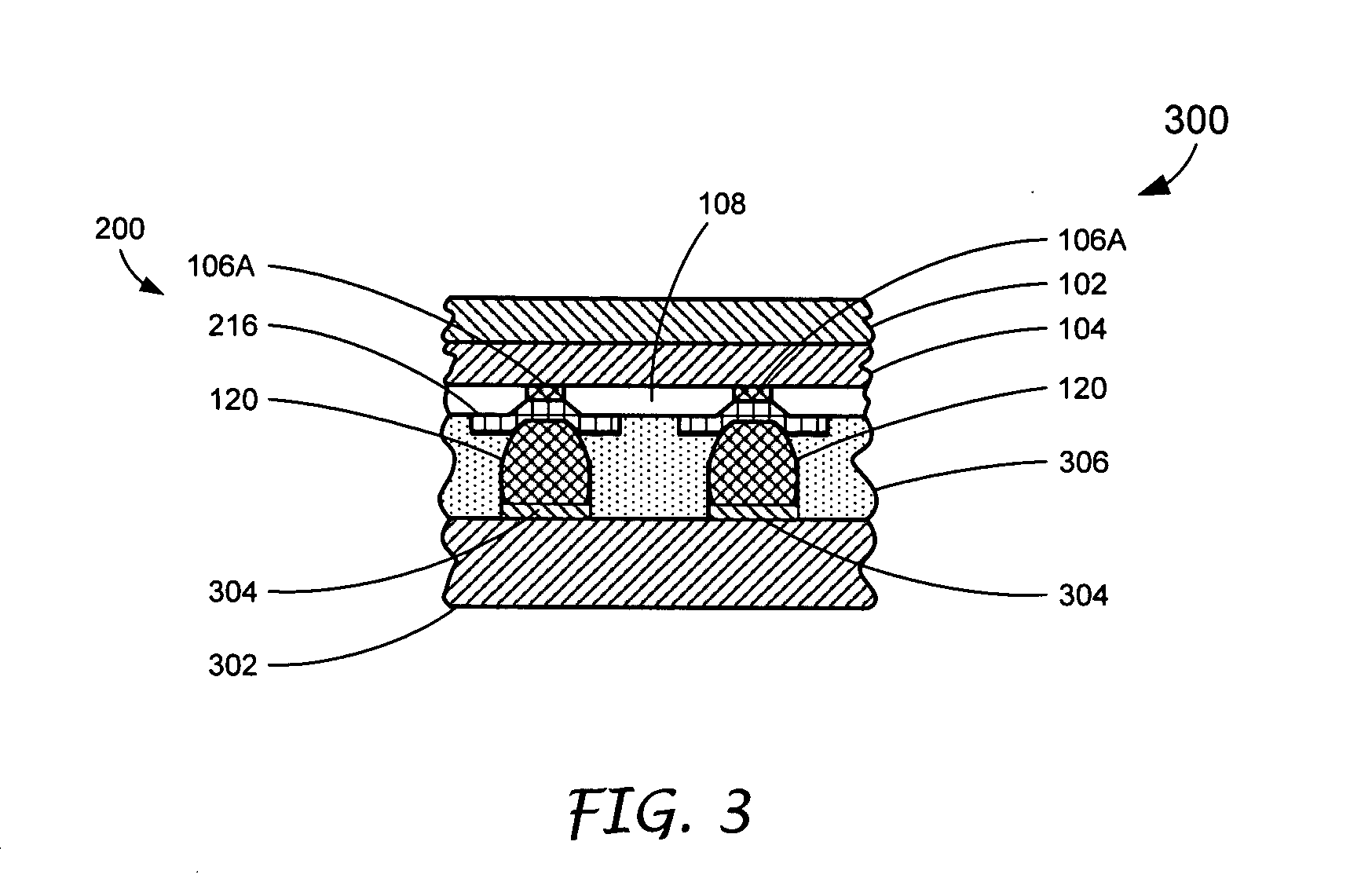
[0014] According to various embodiments of the present invention, an under-bump metallurgy (UBM) may be tailored to meet the requirements of low-stress under the constraints of a specified current carry capability and operating temperature. The UBMs described herein are particularly advantageous in applications where a solder bump is a tin-based solder alloy doped with copper. As noted above, a commonly used thin-film UBM is composed of 4000 angstroms of aluminum, 3500 angstroms of nickel / vanadium and 8000 angstroms of copper. As compared to the present state of prior art UBMs, a factor of three in reduction of film stress may be achieved for a UBM that includes 1000 angstroms of aluminum, 1000 angstroms of nickel / vanadium and 1000 angstroms of copper. According to another aspect of the present invention, a film stress factor reduction of about 15 can be achieved through the use of a UBM that includes 500 angstroms of aluminum and 1000 angstroms of copper.

[0015] As noted above, tin...


PUM


Abstract

An integrated circuit (IC) includes a semiconductor material, electronic circuitry formed on the semiconductor material, a contact layer formed on the electronic circuitry, a final passivation layer formed on the contact layer and an under-bump metallurgy (UBM) formed on at least a portion of the final passivation layer. The contact layer includes a plurality of contacts pads for providing external access to the electronic circuitry. The final passivation layer includes a plurality of windows that extend through the final passivation layer to the contact pads. The UBM includes an aluminum layer having a thickness of about 800 angstroms to about 1200 angstroms, a nickel/vanadium (Ni/V) layer having a thickness of about 800 angstroms to about 1200 angstroms and a copper (Cu) layer having a thickness of about 800 angstroms to about 1200 angstroms.

Description

TECHNICAL FIELD [0001] The present invention is generally directed to an integrated circuit and, more specifically, to an integrated circuit with low-stress under-bump metallurgy that imparts reduced stress. BACKGROUND OF THE INVENTION [0002] For integrated circuits (ICs), such as flip-chips, proper selection of an application appropriate under-bump metallurgy (UBM) is essential, prior to application of a solder bump on a top surface of the flip-chip. In a typical traditional flip-chip, a UBM includes a plurality of metal layers, which are deposited onto a final passivation layer, which includes windows that allow access to input / output (I / O) pads of the flip-chip. In a typical flip-chip, the pads are made of a metal, such as aluminum, and the UBM consists of metal layers, e.g., aluminum (Al), nickel / vanadium (Ni / V) and copper (Cu), which are deposited in successive process steps. A relatively well known thin-film UBM has utilized 4000 angstroms of aluminum, 3500 angstroms of nickel...

Claims


Application Information

Patent Timeline
Patent Type & Authority Applications(United States)
IPC IPC(8): H01L23/48H01L23/52H01L29/40
CPCH01L24/10H01L24/05H01L2224/0401H01L2224/13099H01L2224/16H01L2224/8121H01L2224/81815H01L2224/83102H01L2224/83191H01L2224/92125H01L2924/01013H01L2924/01014H01L2924/01022H01L2924/01028H01L2924/01029H01L2924/01033H01L2924/01046H01L2924/01047H01L2924/0105H01L2924/01074H01L2924/01078H01L2924/01079H01L2924/01082H01L2924/01322H01L2924/01327H01L2924/014H01L2924/05042H01L2924/14H01L2924/30105H01L2924/01006H01L2924/01019H01L2924/01023H01L2924/01024H01L2924/0002H01L24/81H01L24/13H01L2224/05022H01L2224/81011H01L2224/05572H01L2224/05027H01L2924/00014H01L2924/00H01L2224/05552H01L2224/13
Inventor STEPNIAK, FRANKHIGDON, WILLIAM D.
Owner DELPHI TECH INC
Why Eureka
Try Eureka