Memory element and memory

a memory element and memory technology, applied in the field of memory element and memory, can solve problems such as the improvement of spin injection efficiency, and achieve the effects of reducing the amount of current necessary for reversing the magnetization direction of the memory layer in the memory element due to spin injection, reducing the amount of current needed, and ensuring the operation of sufficient margin of error

Inactive Publication Date: 2007-02-08
SONY CORP
View PDF10 Cites 32 Cited by
  • Summary
  • Abstract
  • Description
  • Claims
  • Application Information

AI Technical Summary

Benefits of technology

[0048] In addition, the amount of the current (threshold current) necessary for reversal of the magnetization direction of the memory layer in the memory element due to spin injection can be decreased.
[0049] According to the above-described embodiments of the present invention, the amount of the current (threshold current) necessary for reversal of the magnetization direction of a memory layer can be suppressed, which can reduce the amount of the current necessary for inform

Problems solved by technology

However, when the present inventors actually fabricated the memory element having the above-described structure described in the patent document and checked the properties o

Method used


Image

  • Memory element and memory
  • Memory element and memory
  • Memory element and memory

Examples


working example

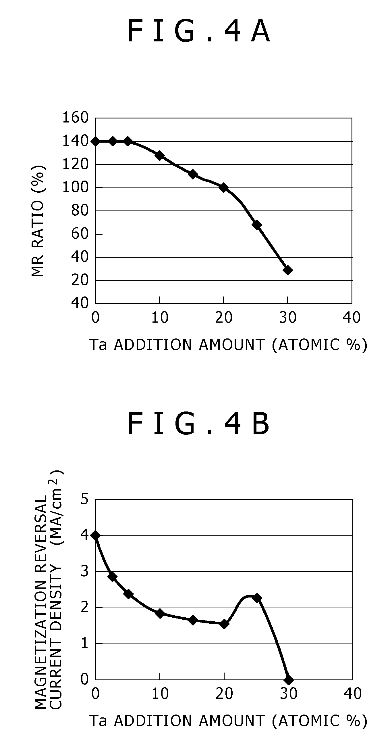
[0195] The materials, film thicknesses, and so on of the respective layers were specifically chosen for the structure of the memory element of the present invention, and the properties of the memory element were investigated.

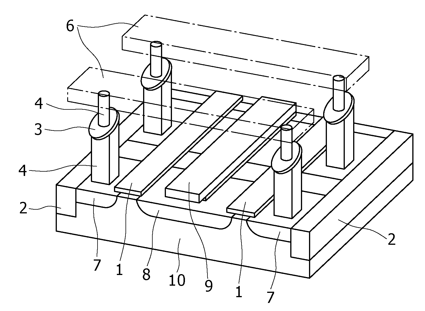
[0196] An actual memory includes, besides memory elements, semiconductor circuits for switching and so on as shown in FIGS. 1 and 6. However, in the working examples, studies were made on a wafer on which memory elements have been formed in order to investigate the magnetoresistance properties of the memory layer.

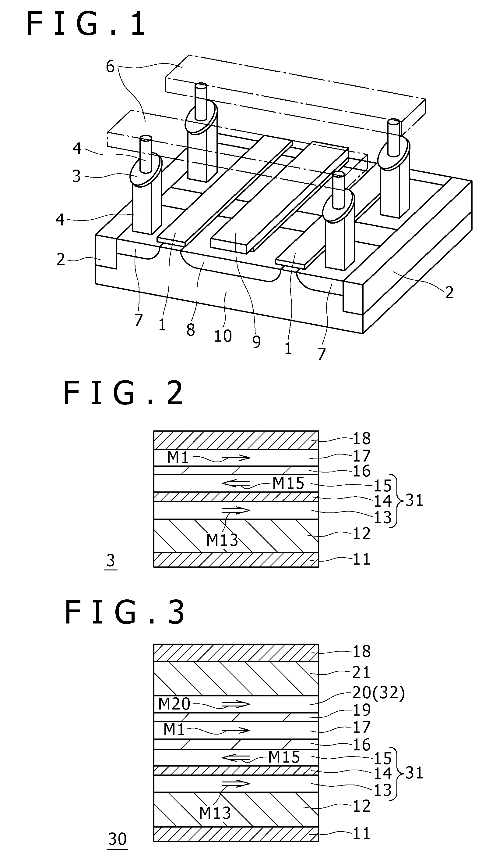
[0197] A thermally oxidized film with a thickness of 300 nm was formed on a silicon substrate with a thickness of 0.725 mm, and then the memory element 3 having the structure of FIG. 2 is formed on the thermally oxidized film.

[0198] The specific materials and film thicknesses of the respective layers in the memory element 3 having the structure shown in FIG. 2 were as follows. The underlying film 11 was formed of a Ta film with a thickness of 3 nm, a...


PUM


Abstract

The present invention provides a memory element including a memory layer that holds information based on a magnetization state of a magnetic substance, and a magnetization pinned layer that is provided for the memory layer with intermediary of an intermediate layer therebetween, the intermediate layer being composed of an insulator. Spin-polarized electrons are injected in a layer-stacking direction to thereby change a direction of magnetization of the memory layer, so that information is recorded in the memory layer. At least one ferromagnetic layer included in the memory layer is composed mainly of CoFeTa, and has Ta content in a range from 1 atomic percent (at %) to 20 at %.

Description

CROSS REFERENCES TO RELATED APPLICATIONS [0001] The present invention contains subject matter related to Japanese Patent Application JP 2005-228902 filed in the Japanese Patent Office on Aug. 5, 2005, the entire contents of which being incorporated herein by reference. BACKGROUND OF THE INVENTION [0002] 1. Field of the Invention [0003] The present invention relates to a memory element that includes a memory layer for storing the magnetization state of a ferromagnetic layer as information and a magnetization pinned layer of which magnetization direction is fixed, and changes the magnetization direction of the memory layer in response to current flow therethrough. The invention also relates to a memory that includes the memory element and is suitably used as a nonvolatile memory. [0004] 2. Description of the Related Art [0005] In information apparatuses such as computers, high speed and high density DRAMs are widely used as a random access memory. [0006] However, the DRAM is a volatil...

Claims


Application Information

Patent Timeline
IPC IPC(8): G11C11/00
CPCG11C11/16H01L43/10H01L27/228H10B61/22H10N50/85
Inventor HOSOMI, MASANORIOHMORI, HIROYUKIKANO, HIROSHI
Owner SONY CORP
Why Eureka
Try Eureka