Method and apparatus for reviewing defects of semiconductor device

a technology for semiconductor devices and defects, applied in the direction of image analysis, image enhancement, electric discharge tubes, etc., can solve the problems of inability to identify the defect part, lots of potential contrast defects, and limited application of this system, so as to prevent erroneous detection of parts, and review defect effectively

Active Publication Date: 2007-02-08
HITACHI HIGH-TECH CORP
View PDF6 Cites 44 Cited by
  • Summary
  • Abstract
  • Description
  • Claims
  • Application Information

AI Technical Summary

Benefits of technology

[0018] According to the invention, the step of taking the reference image of low magnification can be omitted by synthesizing the reference image from the defect image in detection of the defect, resulting in effective review of the defect. It is d...

Problems solved by technology

That is, applications of this system are limited.
Additionally, when there is no corresponding desired reference image among the images prepared, the identification of the defect part is impossible.
In a step of forming holes in manufacturing the semiconductor device, lots of potential contrast defects (which are defects that appear to differ from other parts in brightness by observation with a secondary electron image because the potential of a wir...

Method used


Image

  • Method and apparatus for reviewing defects of semiconductor device
  • Method and apparatus for reviewing defects of semiconductor device
  • Method and apparatus for reviewing defects of semiconductor device

Examples


Embodiment Construction

[0041] Reference will now be made to preferred embodiments of the invention, which are illustrated in the accompanying drawings.

[0042] First Preferred Embodiment

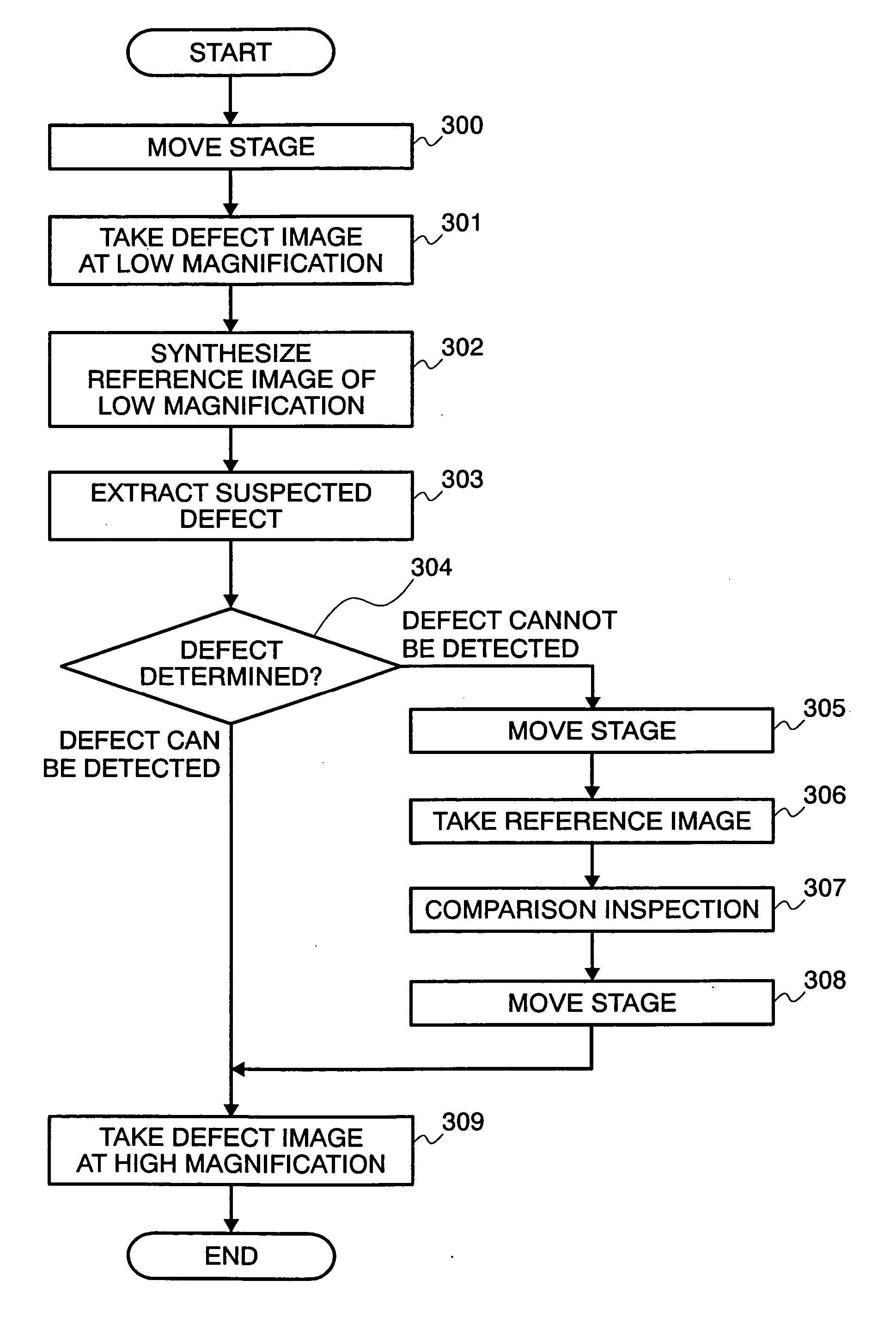
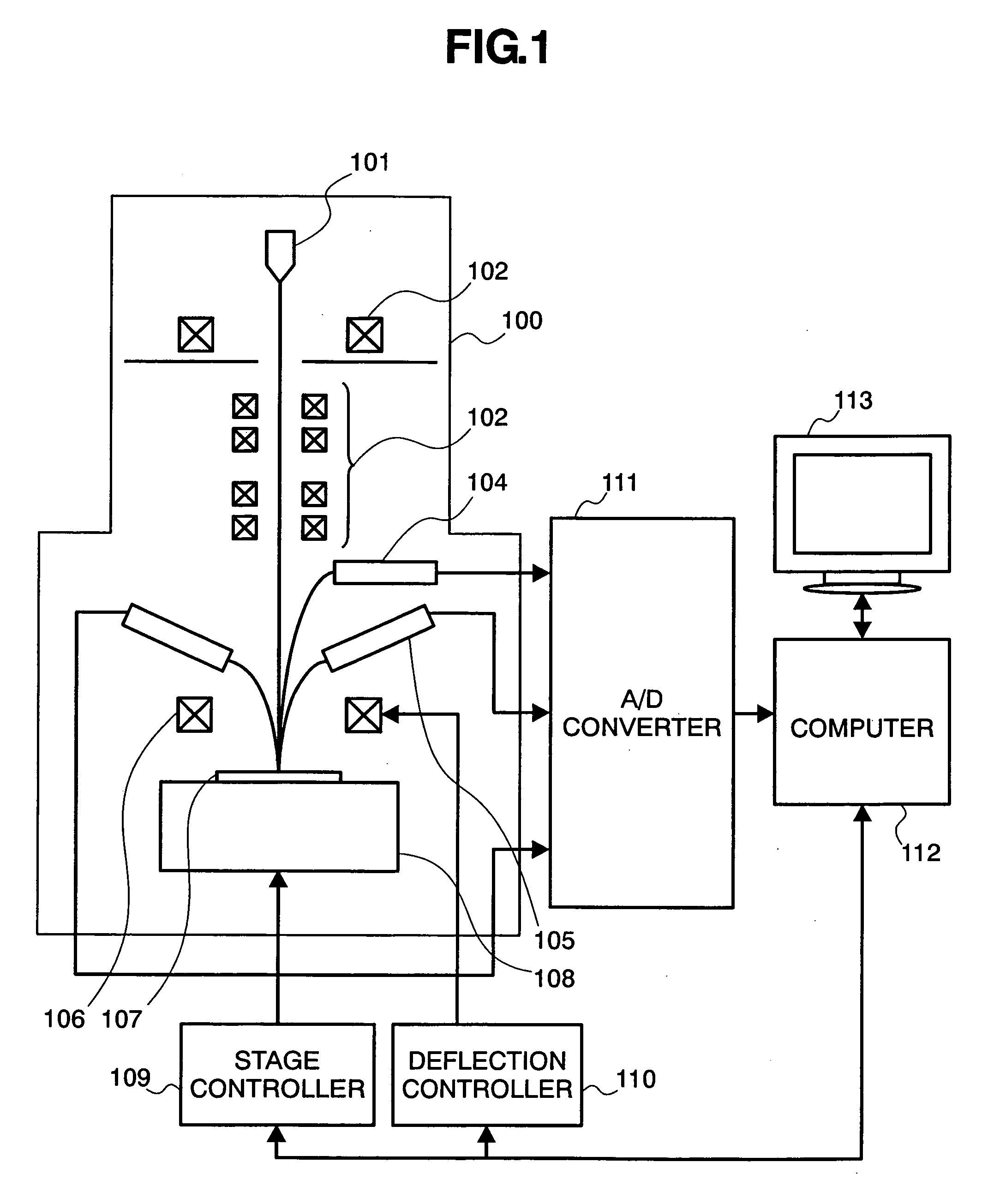
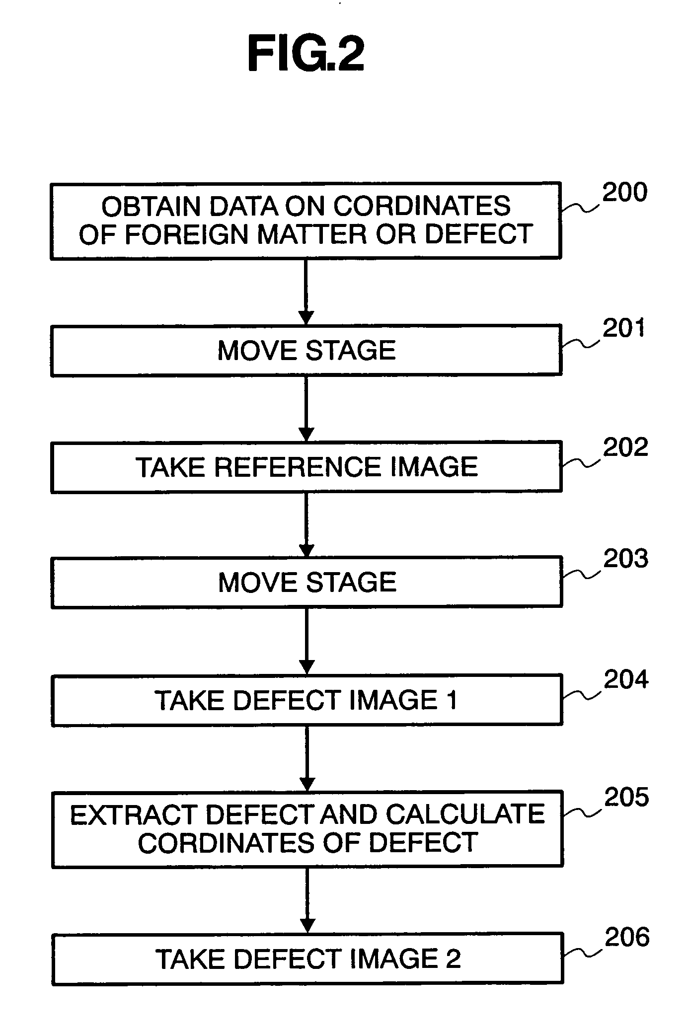
[0043]FIG. 1 shows a schematic diagram of a configuration of a review apparatus using a scanning electron microscope (SEM) for analyzing defects occurring in a semiconductor wafer according to a first preferred embodiment of the invention. An electron optical system of SEM is accommodated in a vacuum chamber 100. Electrons emitted from an electron gun 101 are converged by a focusing lens 102, and directed to an irradiation position by a deflection and scanning coil 103. The electrons then come into a focus on a semiconductor wafer 107 by an objective lens 106 controlled by a deflection controller 110. The irradiation position is moved by an XY stage 108, which is controlled by a stage controller 109. Secondary reflected electrons are emitted from the semiconductor wafer 107, which has been irradiated with the electrons, an...


PUM


Abstract

A method and apparatus for reviewing defects of a semiconductor device is provided which involves detecting a defect on a SEM image taken at low magnification, and reviewing the defect on a SEM image taken at high magnification, and which can review a lot of defects in a short period of time thereby to improve the efficiency of defect review. In the present invention, the method for reviewing defects of a semiconductor device includes the steps of obtaining an image including a defect on the semiconductor device detected by a detection device by use of a scanning electron microscope at a first magnification, making a reference image from the image including the defect obtained at the first magnification, detecting the defect by comparing the image including the defect obtained at the first magnification to the reference image made from the image including the defect at the first magnification, and taking an image of the detected defect at a second magnification that is larger than the first magnification.

Description

BACKGROUND OF THE INVENTION [0001] The invention relates to an apparatus for inspecting appearance of a semiconductor device to review defects thereon. [0002] In a manufacturing process of a semiconductor device, in order to ensure a high yield of products, it is necessary to detect and repair various defects occurring in the process at an early stage. This is normally carried out by the following steps. [0003] A semiconductor wafer of interest to be inspected is inspected by a wafer-appearance inspection system, a wafer foreign matter detection system, or the like, to detect the position of a defect occurring on the wafer, or foreign matter attached thereto. [0004] Then, the defect detected is observed (hereinafter referred to as “review”), and classified according to sources. In this review, a device dedicated for defect review, including a microscope, is normally used to observe or review a defective part at high magnification. In some cases, other devices having a reviewing func...

Claims


Application Information

Patent Timeline
IPC IPC(8): G06K9/00
CPCG06T7/001G06T2207/30148H01J2237/2817H01J37/28H01J37/222
Inventor KURIHARA, MASAKIHONDA, TOSHIFUMINAKAGAKI, RYO
Owner HITACHI HIGH-TECH CORP
Why Eureka
Try Eureka