

Optical waveguide structure
- Summary
- Abstract
- Description
- Claims
- Application Information
AI Technical Summary
Benefits of technology
Problems solved by technology
Method used
Image

Examples
first embodiment
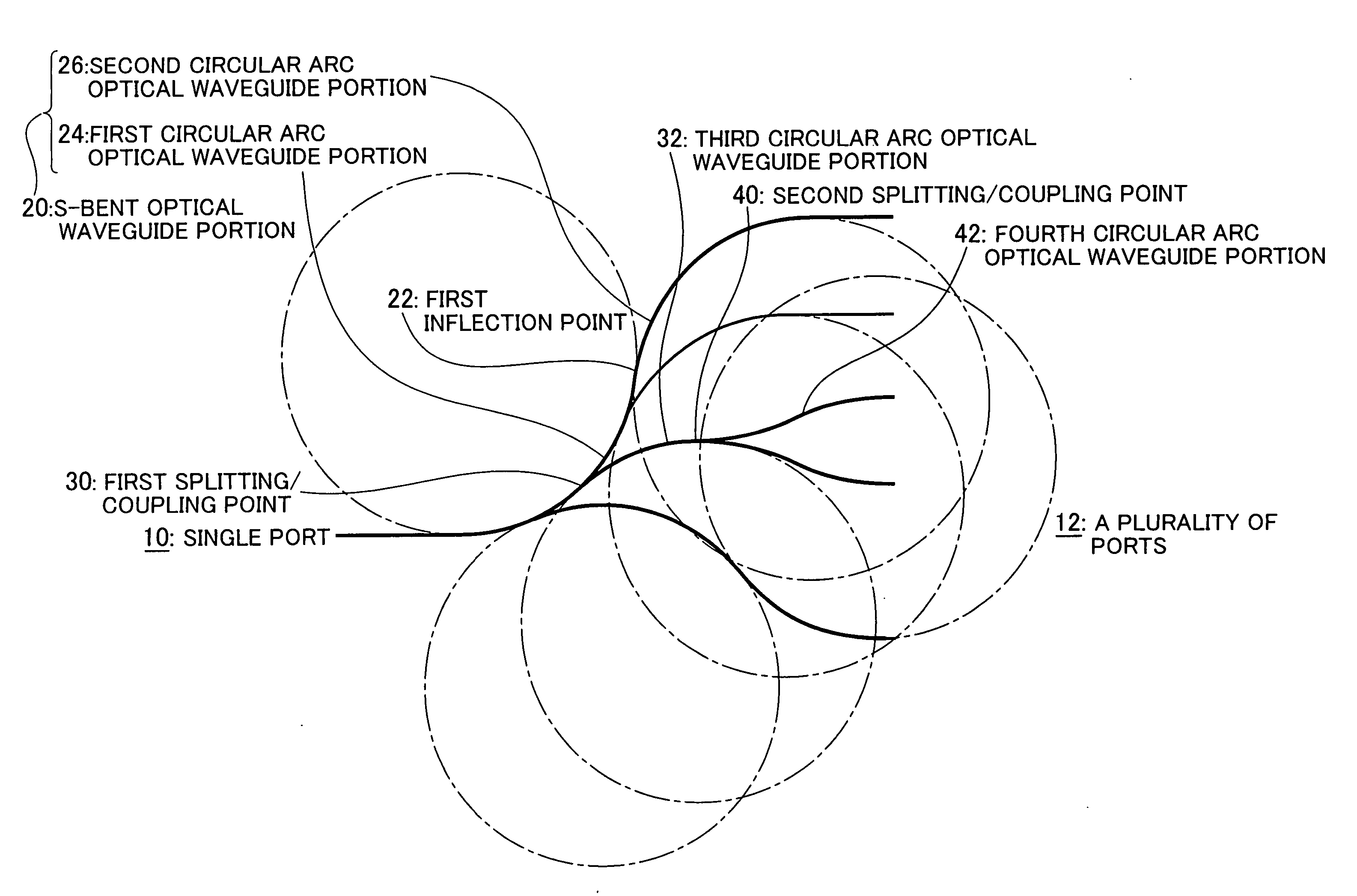
[0077] As shown FIG. 1, an optical waveguide structure of a first embodiment of the present invention is an optical waveguide structure 14 having a single port 10 on one input / output side and a plurality of ports 12 on the other input / output side comprising an S-bent optical waveguide portion 20 arranged on the outermost side of the waveguide structure, tangential lines at opposed ends of the S-bent optical waveguide portion 20 being parallel to each other, the S-bent optical waveguide portion 20 including a first circular arc optical waveguide portion 24 and a second circular arc optical waveguide portion 26 connected thereto at a first inflection point 22 where a curvature of the S-bent optical waveguide portion 20 is inverted, the first circular arc optical waveguide portion 24 having a first splitting / coupling point 30 located on a single-port side relative to the first inflection point 22; and a third circular arc optical waveguide portion 32 extending from the first splitting / ...
second embodiment
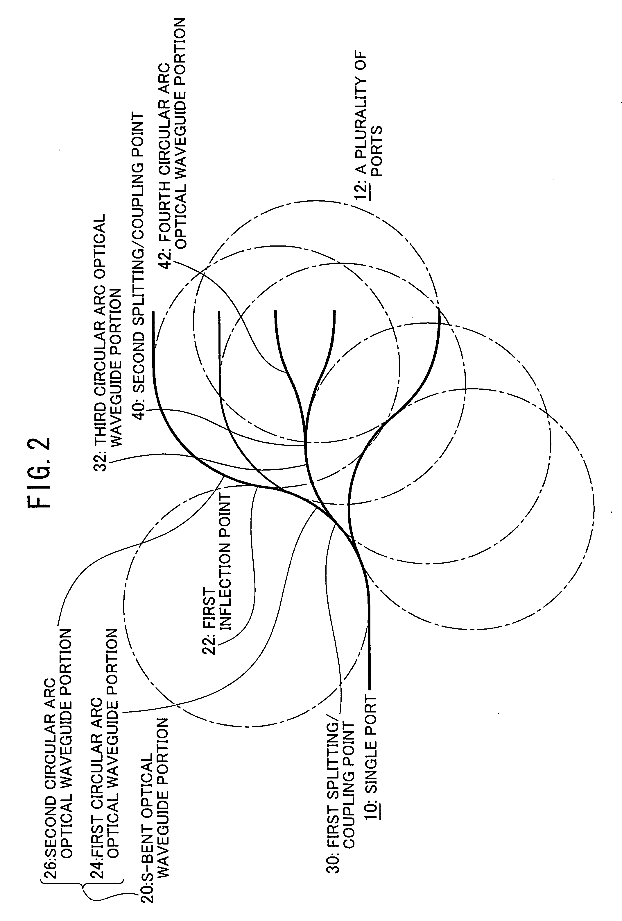
[0078] As shown in FIG. 2, in an optical waveguide structure of a second embodiment of the present invention, the third circular arc optical waveguide portion 32 has a second splitting / coupling point 40; and the waveguide structure further comprises a fourth circular arc optical waveguide portion 42 extending from the second splitting / coupling point 40 toward the plural-ports side 12 and having a curvature inverted relative to the third circular arc optical waveguide portion 32; wherein, at the second splitting / coupling point 40, a tangential line of the third circular arc optical waveguide portion 32 and a tangential line of the fourth circular arc optical waveguide portion 42 are parallel to and spaced from each other.
third embodiment
[0079] As shown in FIG. 3, in an optical waveguide structure of a third embodiment of the present invention, the fourth circular arc optical waveguide portion 42 has a third splitting / coupling point 50; and the waveguide structure further comprises a fifth circular arc optical waveguide portion 60 extending from the third splitting / coupling point 50 toward the plural-ports side 12 and having a curvature inverted relative to the fourth circular arc optical waveguide portion 42; wherein, at the third splitting / coupling point 50, a tangential line of the fourth circular arc optical waveguide portion 42 and a tangential line of the fifth circular arc optical waveguide portion 60 are parallel to and spaced from each other.
[0080] In these embodiments, (a) V-shaped groove(s) for connecting (an) optical fiber(s) to the waveguide may be provided on at least one of the single-port side and the plural-ports side. Providing the V-shaped groove facilitates mounting of an optical fiber to the wa...
PUM
 Abstract
Description
Claims
Application Information