Manufacturing method of an organic electroluminescence device

a manufacturing method and electroluminescence technology, applied in semiconductor devices, solid-state devices, coatings, etc., can solve the problems of difficult to form a pattern with high accuracy, difficult to divide into three colors of rgb, and poor pattern accuracy, so as to achieve high production efficiency and high accuracy

Inactive Publication Date: 2007-02-08
TOPPAN PRINTING CO LTD
View PDF12 Cites 7 Cited by
  • Summary
  • Abstract
  • Description
  • Claims
  • Application Information

AI Technical Summary

Benefits of technology

[0028] Process of manufacture of the organic electroluminescence device which organic luminous layer is formed by a printing method with the use of organic luminescent ink including an organic solvent is provided in the present invention. Ar

Problems solved by technology

When a substrate for formation of thin film upsizes, in resistance heat coating by vaporization method, accuracy of the pattern becomes worse.
But in the wet coating method, it is difficult to form a pattern with high accuracy.
In addition, it is difficult to divide into three colors of RGB when RGB liquids are coated.
Therefore method to use metal hard printing plate lik

Method used


Image

  • Manufacturing method of an organic electroluminescence device
  • Manufacturing method of an organic electroluminescence device
  • Manufacturing method of an organic electroluminescence device

Examples


example 1

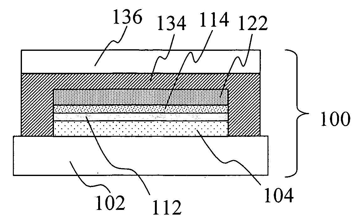
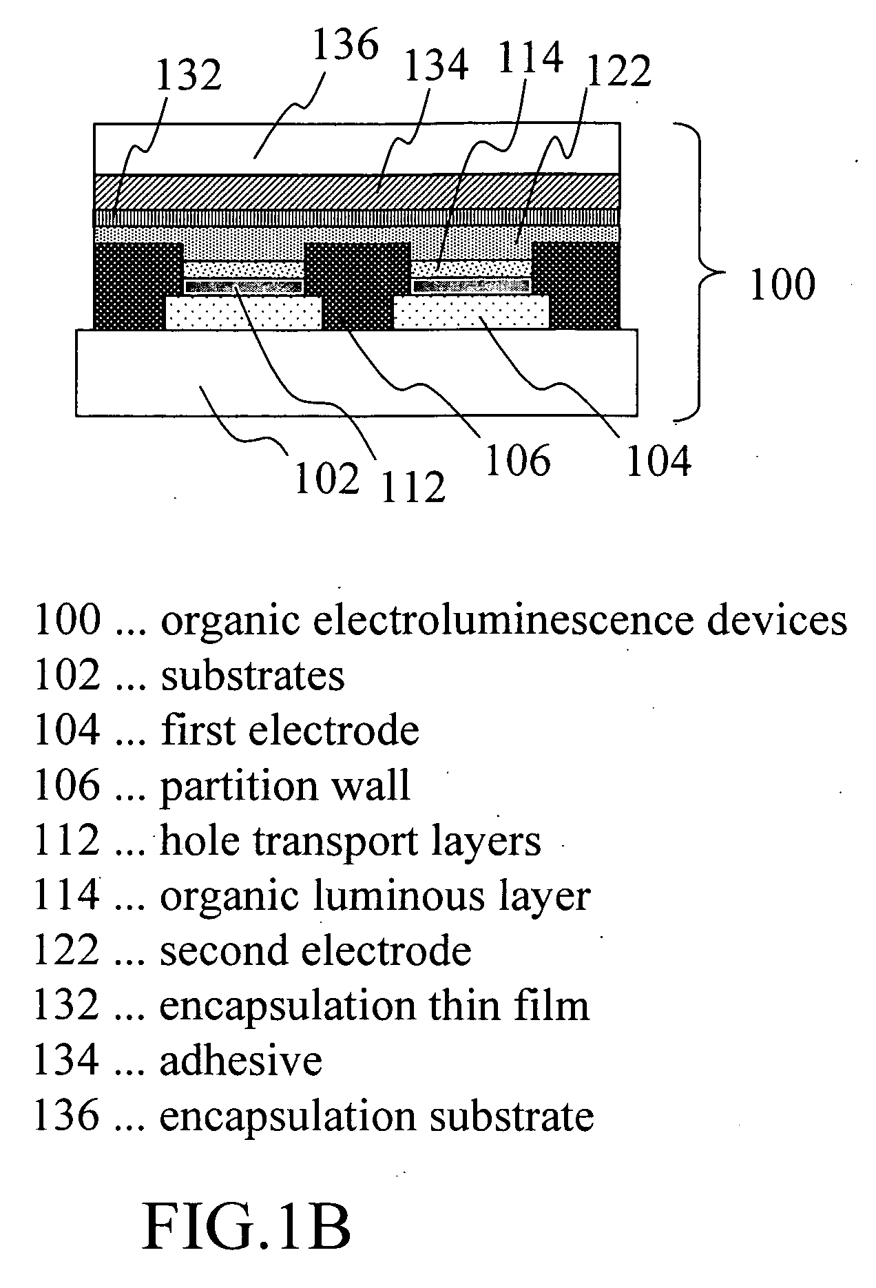
[0133] Thin film of an indium-tin oxide (ITO) which was first electrode was formed to a glass substrate. The first electrode was configuration of stripe. Length of stripe was 33 mm. Line width of stripe was 126 μm. There were 192 stripes, and line space was 40 μm. This was a size of a passive matrix type display unit of diagonal 1.8 inches.

[0134] Subsequently coating liquid was applied to the glass substrate by a spin coating, which formed stripe-shaped first electrode. And the unnecessary region which was not necessary for a luminescent was wiped, and it was removed. And drying by heating was done, and, in this way, a hole transport layer was formed. The coating liquid was the coating fluid which dissolved 3,4-polyethylenedioxithiophene (PEDOT) as a hole transport material in pure water. The substrate that organic luminous layer would be printed was prepared in this way.

[0135] For organic luminescent ink, the liquor which dissolved the polyphenylene vinylene derivative which was ...


PUM

PropertyMeasurementUnit
Heightaaaaaaaaaa
Heightaaaaaaaaaa
Lengthaaaaaaaaaa

Abstract

An organic electroluminescence device manufacturing method is disclosed wherein the device comprises a substrate, a first and second electrode, and an organic luminous layer. The method comprising: hardening of a water development type photosensitive resin to form a plastic plate; and printing organic luminescent ink on a substrate by relief printing method with the use of the plastic plate, wherein the organic luminescent ink is an ink capable of scattering organic luminescent material in an organic solvent.

Description

CROSS REFERENCE [0001] This application claims priority to Japanese application number 2005-063434, filed on Mar. 3, 2005, which is incorporated by reference. BACKGROUND OF THE INVENTION [0002] 1. Field of the Invention [0003] The present invention is related to process of manufacture an organic electroluminescence device including an organic luminescent material in a luminous layer. [0004] More particularly, the present invention is related to process of manufacture an organic electroluminescence device by means of relief printing method. [0005] 2. Description of the Related Art [0006] An organic electroluminescence device has an organic luminous layer including organic luminescent material between two opposed electrodes. It emits light by electric current to the organic luminous layer. Film thickness of the luminous layer is important, and it is necessary to make the film of around 100 nm to emit light efficiently. Even more particularly, it is necessary to form the luminous layer...

Claims


Application Information

Patent Timeline
IPC IPC(8): B05D5/12B05D5/00
CPCH01L27/3295H01L51/0004H01L51/56H01L51/0038H01L51/0037H10K59/122H10K59/173H10K71/13H10K85/114H10K85/1135H10K71/00
Inventor TAKESHITA, KOJISHIMIZU, TAKAHISAKAWAKAMI, HIRONORI
Owner TOPPAN PRINTING CO LTD
Why Eureka
Try Eureka