Semiconductor integrated circuit device
a technology of integrated circuit devices and semiconductors, applied in logic circuits using specific components, pulse techniques, instruments, etc., can solve problems such as cost rise, and achieve the effect of raising the degree of integration of semiconductor integrated circuit devices
- Summary
- Abstract
- Description
- Claims
- Application Information
AI Technical Summary
Benefits of technology
Problems solved by technology
Method used
Image

Examples
first embodiment
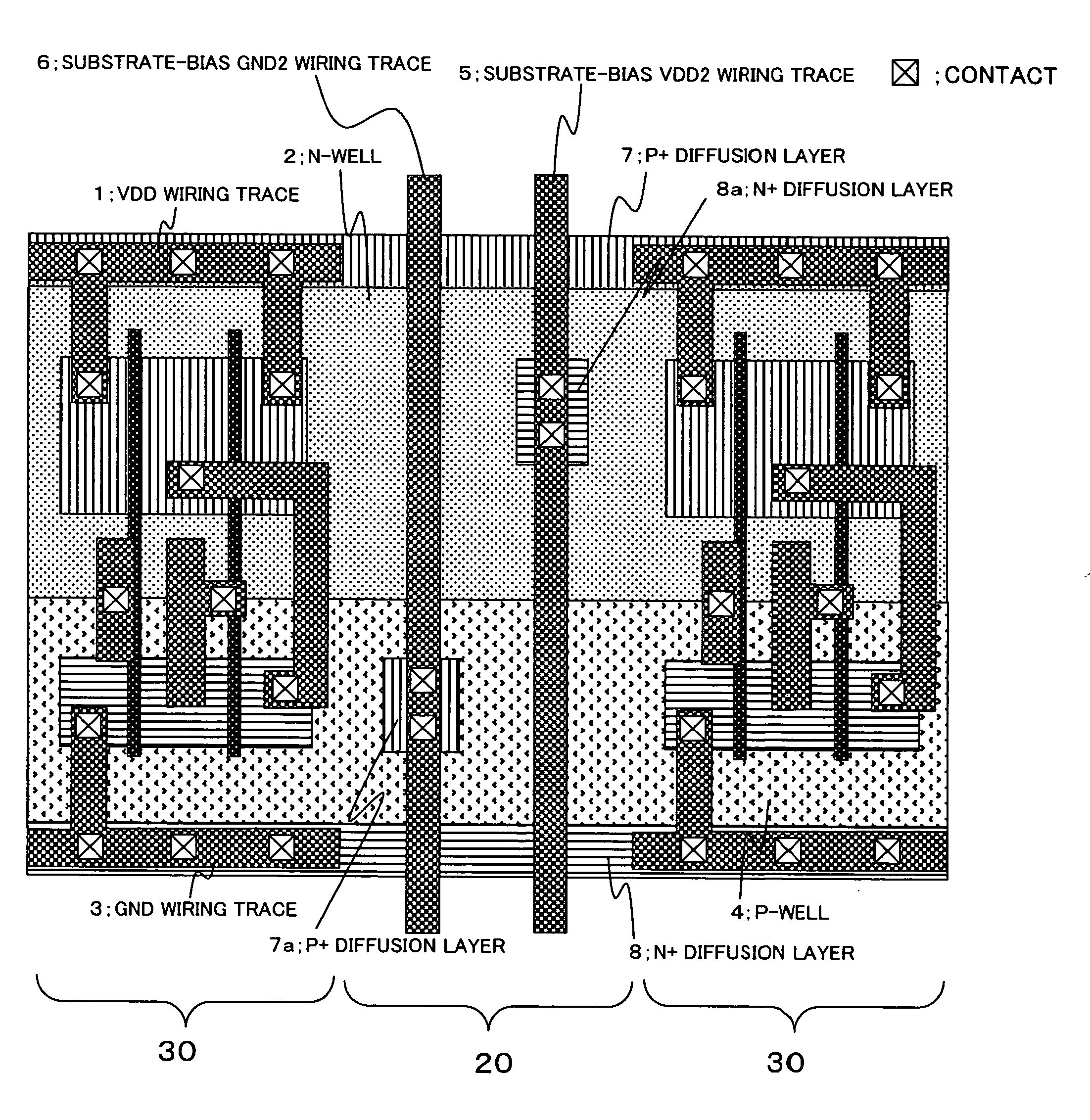
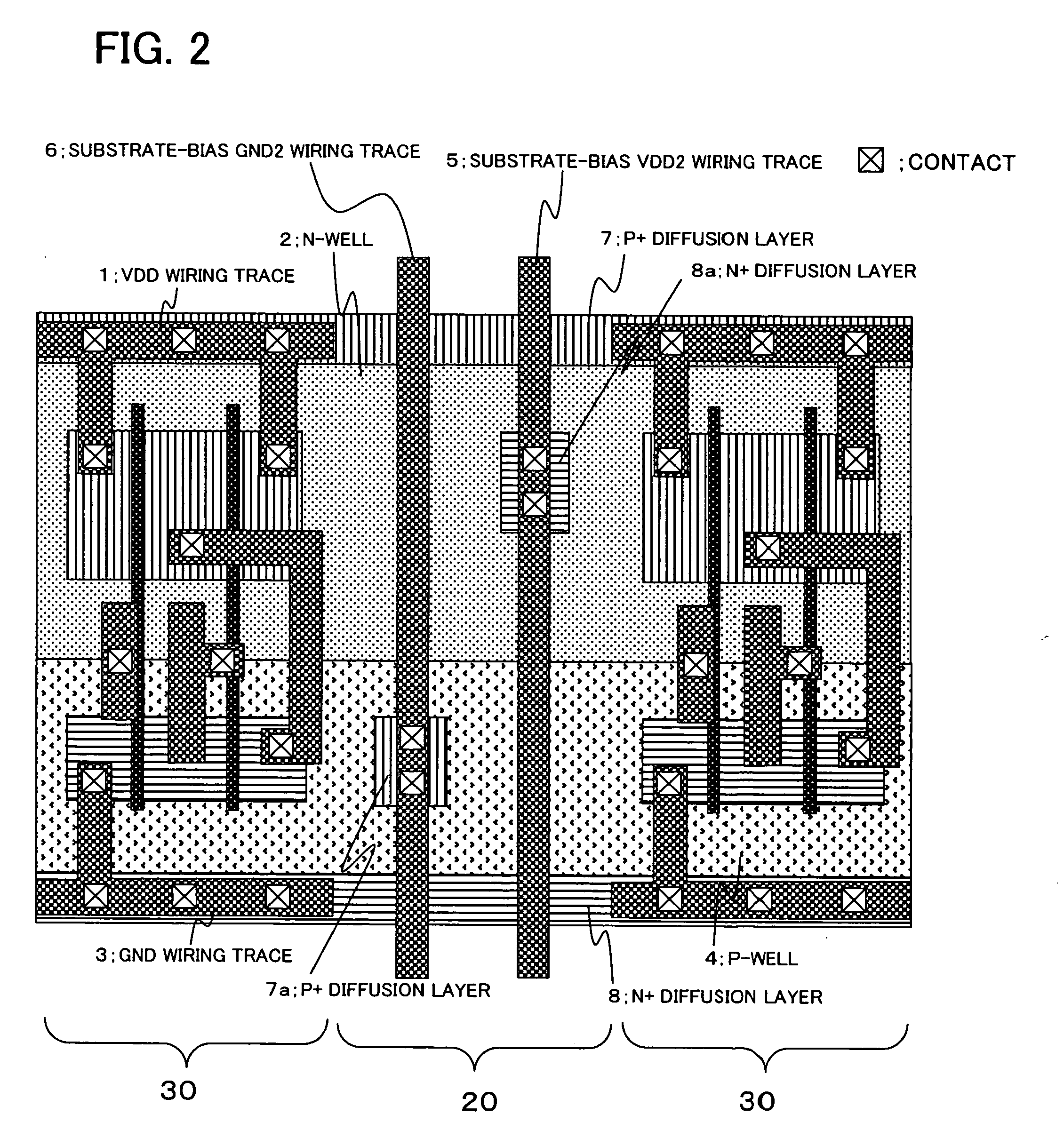
[0039]FIG. 2 is a plan view illustrating the partial structure of a semiconductor integrated circuit device according to a first embodiment of the present invention. As shown in FIG. 2, the semiconductor integrated circuit device has a substrate-bias supply cell 20 and standard cells 30 arranged in a row in the horizontal direction in FIG. 2 astride the N-well 2 and P-well 4. Among the multiplicity of cells that exist in the semiconductor integrated circuit device, two standard cells 30 and the substrate-bias supply cell 20 bracketed by the standard cells 30 are illustrated. In the semiconductor integrated circuit device thus constructed, the VDD wiring trace 1, GND wiring trace 3, substrate-bias VDD2 wiring trace 5 and substrate-bias GND2 wiring trace 6 are routed in the same metal layer, the substrate-bias VDD2 wiring trace 5 and substrate-bias GND2 wiring trace 6 are routed in the vertical direction in the substrate-bias supply cell 20, and the VDD wiring trace 1 and GND wiring t...
second embodiment
[0046]FIGS. 5A and 5B are plan views illustrating the structures of substrate-bias supply cells according to a second embodiment of the present invention, in which FIG. 5A is a plan view of a substrate-bias supply cell 20a for supplying the substrate-bias VDD2 power-supply potential and FIG. 5B a plan view of a substrate-bias supply cell 20b for supplying the substrate-bias GND2 ground potential. The substrate-bias supply cell 20a of FIG. 5A has a structure similar to that of the right half of the substrate-bias supply cell 20 shown in FIGS. 4A and 4B, and the substrate-bias supply cell 20b of FIG. 5B has a structure similar to that of the left half of the substrate-bias supply cell 20 shown in FIGS. 4A and 4B.
[0047] More specifically, the substrate-bias supply cell 20a in FIG. 5A applies bias voltage to the N-well 2 and exists in a structure in which the N-well 2 and P-well 4 are formed on the semiconductor substrate. The P+ diffusion layer 7 similar to that of the standard cell 3...
third embodiment
[0052]FIGS. 7A and 7B are plan views illustrating the structures of substrate-bias supply cells according to a third embodiment of the present invention, in which FIG. 7A is a plan view of a substrate-bias supply cell 20c for supplying the substrate-bias VDD2 power-supply potential and FIG. 7B a plan view of a substrate-bias supply cell 20d for supplying the substrate-bias GND2 ground potential. The substrate-bias supply cell 20c of FIG. 7A further constructs a transistor on the P-well 4 in comparison with the substrate-bias supply cell 20a illustrated in FIG. 5A, and the substrate-bias supply cell 20d of FIG. 7B further constructs a transistor on the N-well 2 in comparison with the substrate-bias supply cell 20b illustrated in FIG. 5B.
[0053] More specifically, the substrate-bias supply cell 20c in FIG. 7A is such that part of the N+ diffusion layer 8 formed in the P-well 4 branches in a U-shaped configuration toward the N-well 2 and a gate electrode 15c is disposed on the N+ diffu...
PUM
 Abstract
Description
Claims
Application Information
 - Generate Ideas
- Intellectual Property
- Life Sciences
- Materials
- Tech Scout
- Unparalleled Data Quality
- Higher Quality Content
- 60% Fewer Hallucinations
Browse by: Latest US Patents, China's latest patents, Technical Efficacy Thesaurus, Application Domain, Technology Topic, Popular Technical Reports.
© 2025 PatSnap. All rights reserved.Legal|Privacy policy|Modern Slavery Act Transparency Statement|Sitemap|About US| Contact US: help@patsnap.com