
Using rows/columns of micro-vias to create PCB routing channels in BGA interconnect grid (micro-via channels)

Inactive Publication Date: 2007-02-15
ALCATEL LUCENT SAS
View PDF3 Cites 15 Cited by
  • Summary
  • Abstract
  • Description
  • Claims
  • Application Information

AI Technical Summary

Benefits of technology

[0011] The object of the present invention is to provide an improved PCB and BGA package using rows / columns of micro-vias to create printed wiring boards (PWB) routing channels in a BGA that couple with BGA interconnect vias. Simple patterns, created through the intelligent reconfiguration of printed circuit board interconnect structures have been defined, which permit an increase in escape densities that in turn enable the routing of area array devices in fewer layers. These patterns provide a novel combination of through and micro-via interconnects which leverage the strength of each of these interconnects in unison to achieve a routing capability which would not be realizable with either of these interconnects when used in the customary way.
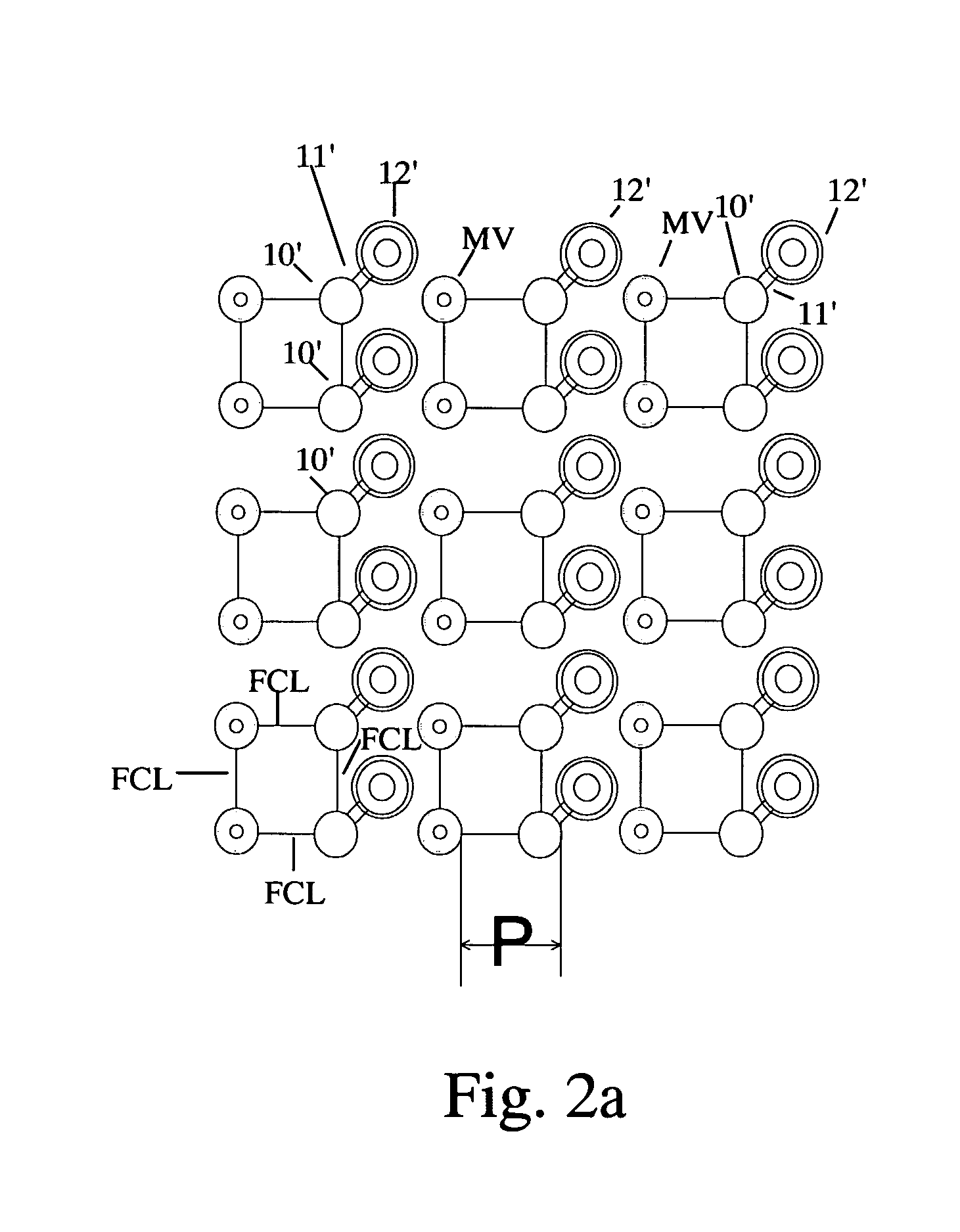
[0012] By creating columns / rows of micro-vias interspersed with columns / rows of regular through-vias as frequently as every second row, columns and rows of through-vias can be eliminated in these locations. As a result, routing channels are created on the first internal layer of the printed circuit board. These channels have several properties which favor the densification of routing: They are wider than the channels that would be created using conventional through-via routing channels, thereby enabling the passage of a greater number of traces. Additionally, the micro-vias employed in this invention cease to exist on the first internal layer, meaning that half of the interconnect is eliminated on all subsequent layers, thinning the interconnect to half of its original density in those areas where this technique is employed. As a result, the interconnect pitch (P) on the surface of the PWB which must be equal to that of the BGA is widened to 2P on all subsequent layers, greatly increasing the routing capacity in these areas.
[0013] While in theory any pinout configuration can be accommodated by this invention, in practice it is preferred to route power and ground connections with through-vias, leaving the micro-vias for the signal carrying connections. Given that every second via is designated a through-via, the limitation that this preference imposes on a given pinout is not overly burdensome.

Problems solved by technology

Finally, at the other extreme, area array technology is following a design trend towards higher pin counts (>2500) and finer pitches (<0.8 mm) which may not be usable at all, without improved routing solutions like the one disclosed herein.
The prior art solution places additional constraints on the pinout configuration of the area array device power and ground pins, which require a high degree of adherence to a specific pinout pattern which in the extreme may not be achievable by certain area array packaging styles.
In general these added constraints are undesirable from a signal integrity standpoint.
Furthermore, that solution involves the sharing of adjacent power and ground pins which is also an unfavorable practice due to the negative impact that it might have on device functionality.

Method used


Image

  • Using rows/columns of micro-vias to create PCB routing channels in BGA interconnect grid (micro-via channels)
  • Using rows/columns of micro-vias to create PCB routing channels in BGA interconnect grid (micro-via channels)
  • Using rows/columns of micro-vias to create PCB routing channels in BGA interconnect grid (micro-via channels)

Examples


Embodiment Construction

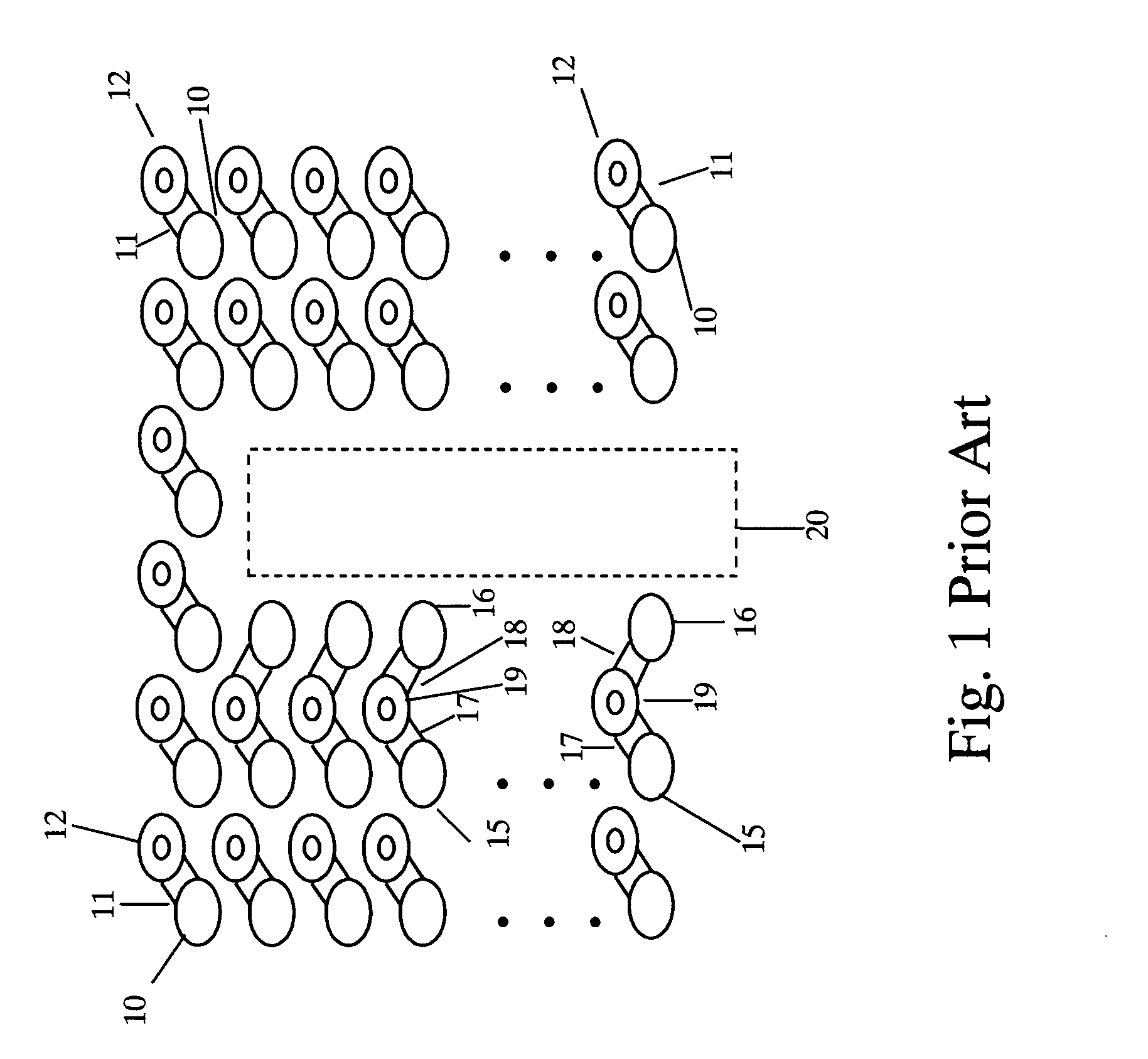
[0021]FIG. 1 is a top view of a surface layer of a printed circuit board (PCB) incorporating one prior art solution. Ball grid array (BGA) ball contact pads 10 are linked by links 11 to through-board vias 12. In order to provide a routing channel 20, selected rows of ball contact pads 15 and 16 are connected through links 17 and 18 to common through-board vias 19 which are designated herein as shared through-board vias. See the above discussion for the disadvantages of this solution.

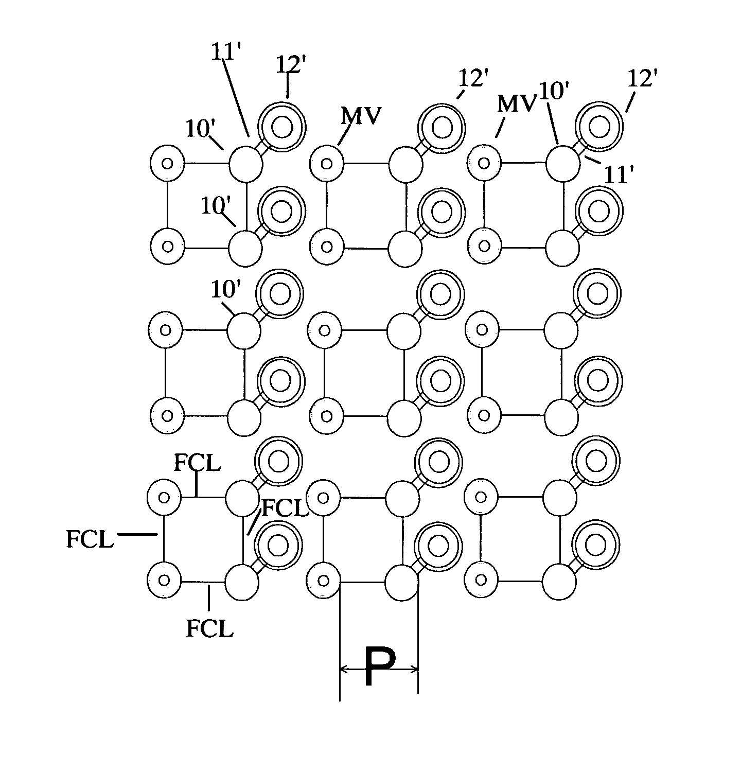
[0022] The present invention is illustrated in FIGS. 2a, 2b and 2c. (The elements with prime numerals correspond to elements in FIG. 1.) The first three circuit board layers are shown to illustrate the requirements of the BGA package.

[0023] By creating columns and / or rows of micro-vias interspersed with columns / rows of regular through vias as frequently as every second column or row, columns and rows of through-vias can be eliminated in these locations. In FIG. 2a, columns of micro-vias MVC1, MVC2, MVC...


PUM


Abstract

A printed circuit board having micro-vias used to connect a portion of the contacts in a selected row or column to the first internal layer of the board, thereby creating routing channels on the second and subsequent internal layers of the board between selected rows or columns of through-board vias used to connect the remaining contacts and a BGA package adapted to be used with the printed circuit board.

Description

REFERENCE TO RELATED APPLICATIONS [0001] The present application is related to the following U.S. patent applications which are assigned to the assignee hereof: [0002] Ser. No. 10 / 991,360 filed Nov. 19, 2004, inventor Paul Brown entitled OFF-WIDTH PITCH FOR IMPROVED CIRCUIT CARD ROUTING; and [0003] Ser. No. 11 / 041,727 filed Jan. 25, 2005, inventor Alex Chan entitled OFF-GRID DECOUPLING OF BALL GRID ARRAY (BGA) DEVICES.BACKGROUND OF THE INVENTION [0004] This invention relates to increasing the efficiency with which signals from area array packages (BGAs and CGAs) are extracted and routed on the printed circuit boards (PCB or circuit card) on which these devices are mounted. [0005] It is well established that the increase in area array connections (pin count) translates to an increase in the number of printed circuit board routing layers needed to support the device escape and routing circuits. The incentive for further increases in routing efficiency stem from the cost and complicati...

Claims


Application Information

Patent Timeline
IPC IPC(8): H05K1/11
CPCH01L23/49816H01L23/49827H01L23/49838H01L23/50H05K1/114H05K3/429H01L2924/0002H05K2201/09227H05K2201/09509H05K2201/10734H01L2924/00
Inventor BROWN, PAUL JAMES
Owner ALCATEL LUCENT SAS
Learn More