

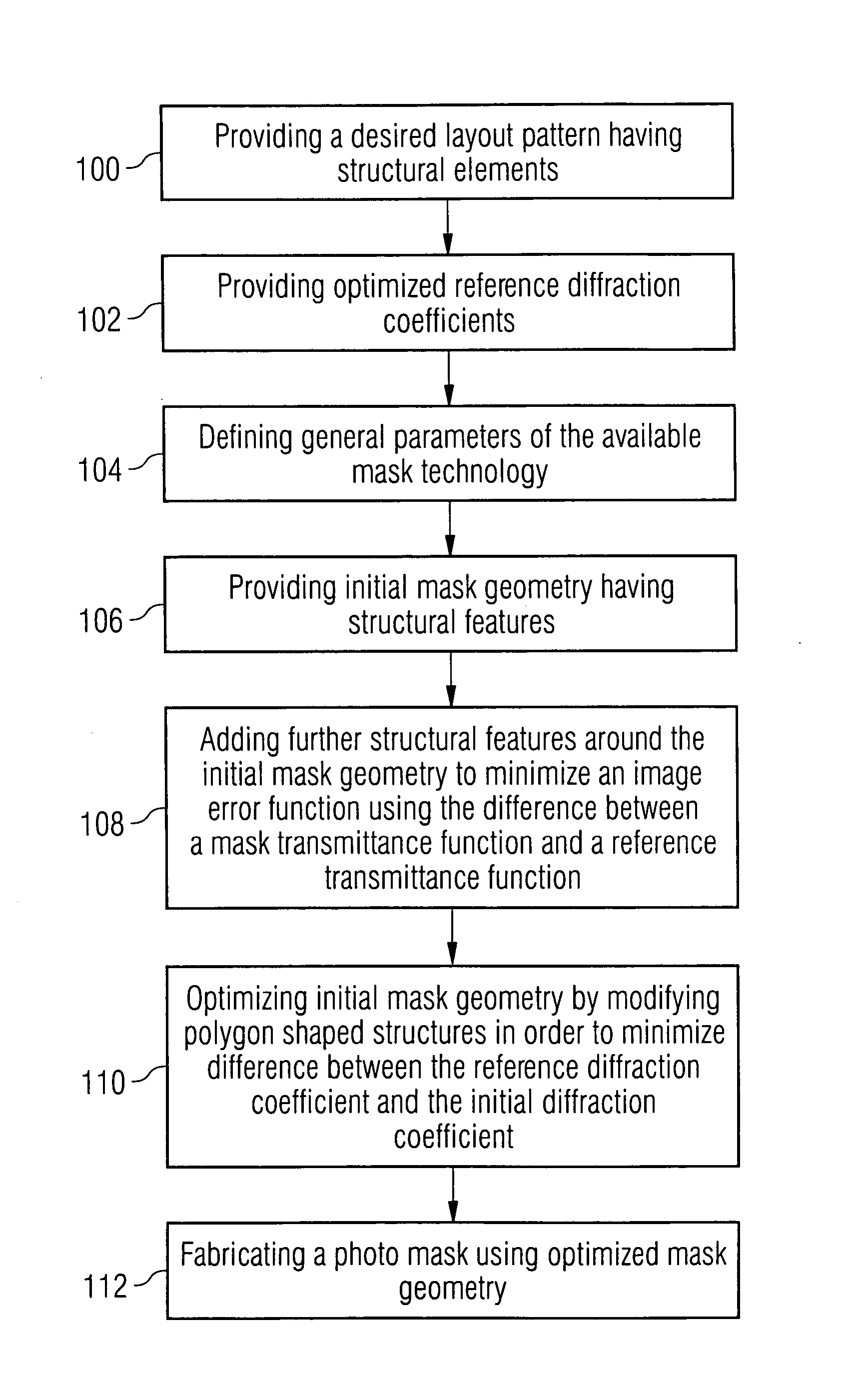
Method for optimizing a photolithographic mask
a photolithographic mask and optimization technology, applied in the field of photolithographic processing, can solve the problems process of optimizing as a feedback problem, and affecting the image quality of isolated structures, etc., and achieve the effect of reducing optimization tim
- Summary
- Abstract
- Description
- Claims
- Application Information
AI Technical Summary
Benefits of technology
Problems solved by technology
Method used
Image

Examples
Embodiment Construction
[0032] A presently preferred embodiment of the methods and the lithographic system according to the invention is discussed in detail below. It is appreciated, however, that the present invention provides many applicable inventive concepts that can be embodied in a wide variety of specific contexts. The specific embodiments discussed are merely illustrative of specific ways to apply the method and the system of the invention, and do not limit the scope of the invention.
[0033] In the following, embodiments of the method and the system are described with respect to improving dimensional accuracy during lithographic projection of a layer of an integrated circuit. The invention, however, might also be useful for other products, e.g., liquid crystal panels or the like.
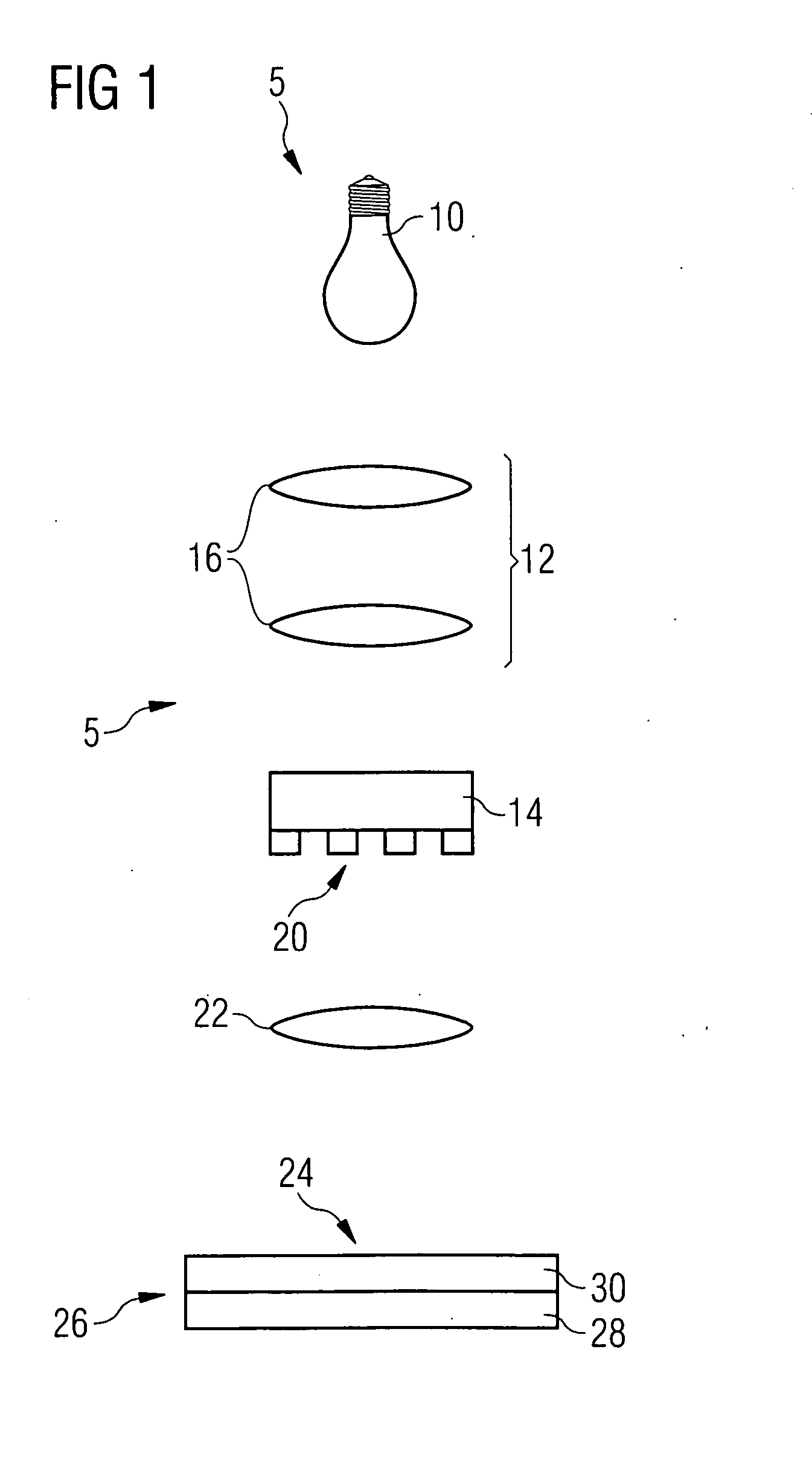
[0034] With respect to FIG. 1, a set-up of a lithographic projection apparatus 5 in a side view is shown. It should be appreciated that FIG. 1 merely serves as an illustration, i.e., the individual components shown in FIG....
PUM
 Abstract
Description
Claims
Application Information