

Ion trap in a semiconductor chip
a technology of semiconductor chips and traps, applied in the field of ion traps, can solve the problems of gate in this impulsive way, not yet demonstrated experimentally, and the own challenges
- Summary
- Abstract
- Description
- Claims
- Application Information
AI Technical Summary
Benefits of technology
Problems solved by technology
Method used
Image

Examples
Embodiment Construction
[0050] The following description of the preferred embodiment(s) is merely exemplary in nature and is in no way intended to limit the invention, or uses.
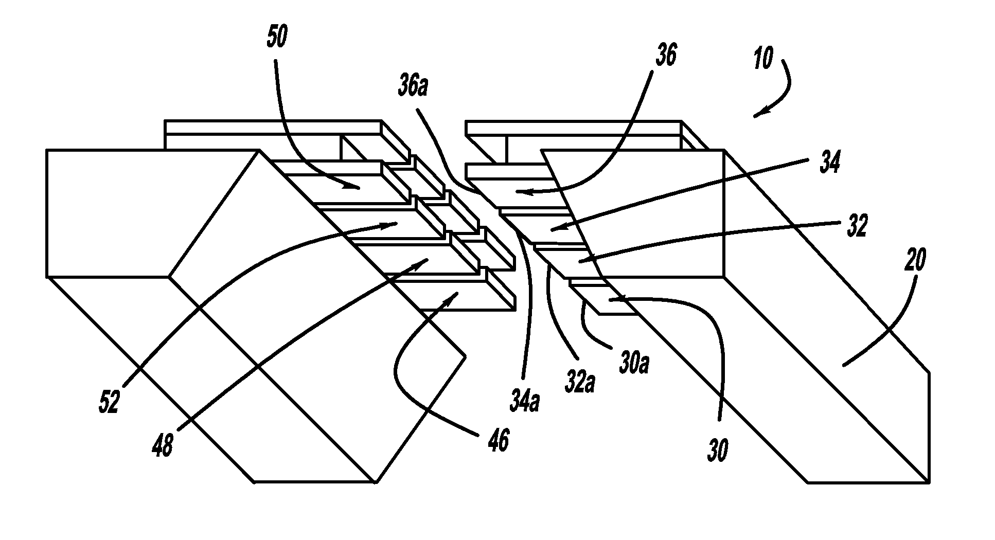
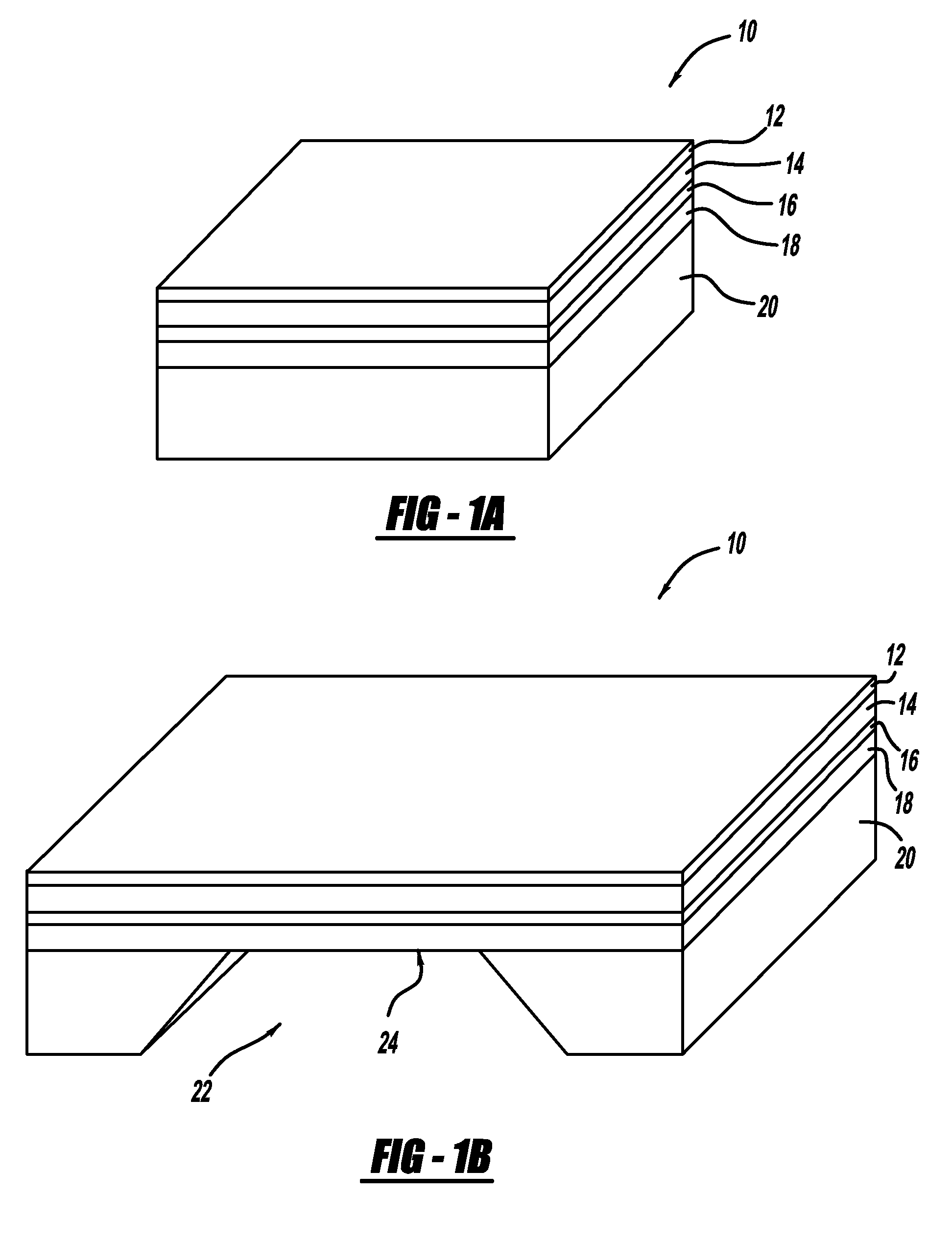
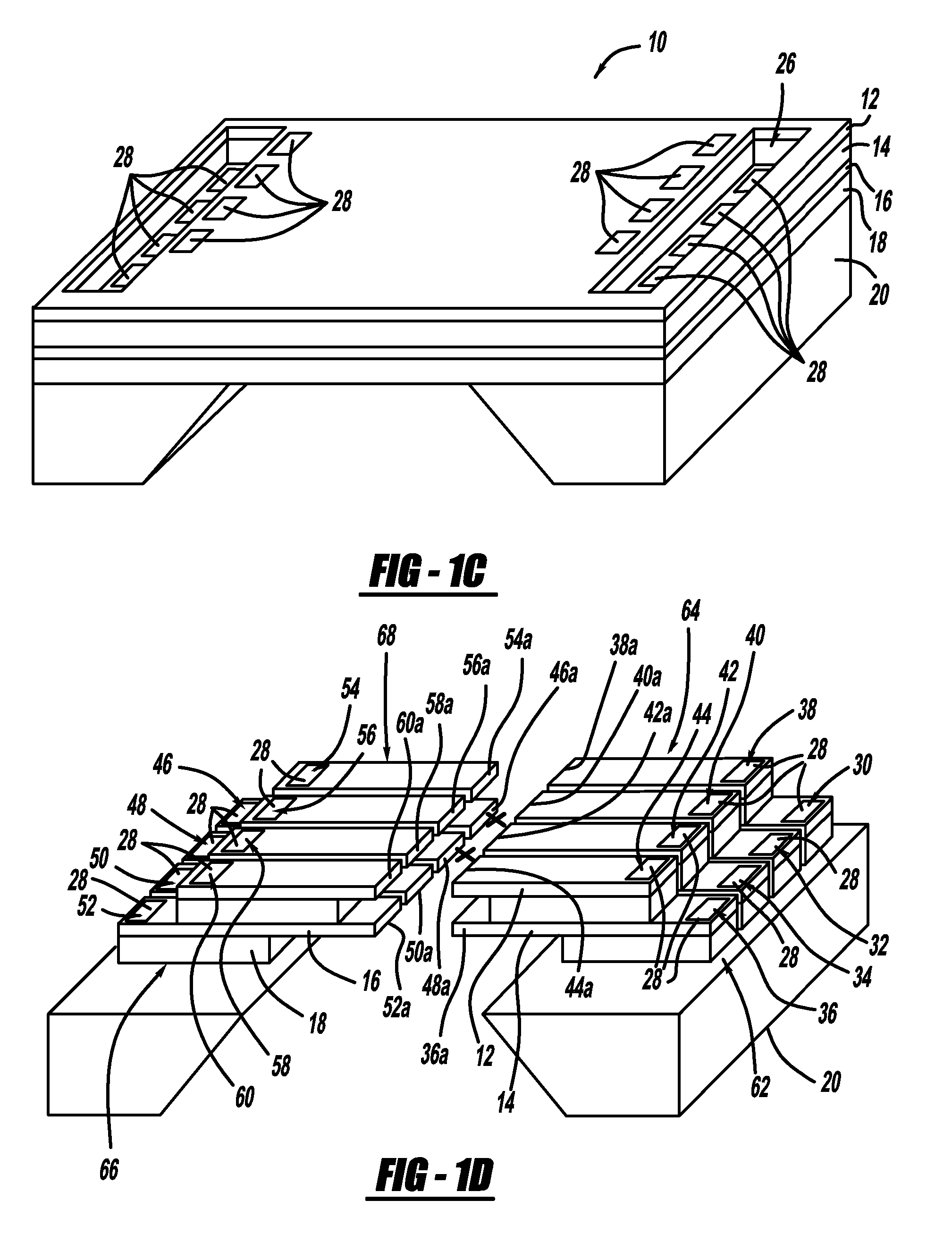
[0051] A micrometer-scale ion trap, fabricated on a monolithic chip using semiconductor micro-electromechanical systems (MEMS) technology, is provided. The present invention confines, allows for laser cooling, laser cools, and measures heating of a single 111Cd+ ion in an integrated radiofrequency trap etched from a doped gallium arsenide (GaAs) heterostructure. Compared with “chip traps” for confining neutral atoms, ion traps of the present invention with similar dimensions and power dissipation offer much higher confinement forces and allow unparalleled control at the single-atom level.
[0052] More specifically, the present invention confines single 111Cd+ qubit ions in a radiofrequency linear ion trap on a semiconductor chip by applying a combination of static and oscillating electric potentials to integrated electrodes. By way o...
PUM
| Property | Measurement | Unit |
|---|---|---|
| drive frequency | aaaaa | aaaaa |
| length | aaaaa | aaaaa |
| delay time | aaaaa | aaaaa |
Abstract
Description
Claims
Application Information