

Reference buffer with improved drift
- Summary
- Abstract
- Description
- Claims
- Application Information
AI Technical Summary
Benefits of technology
Problems solved by technology
Method used
Image

Examples
Embodiment Construction
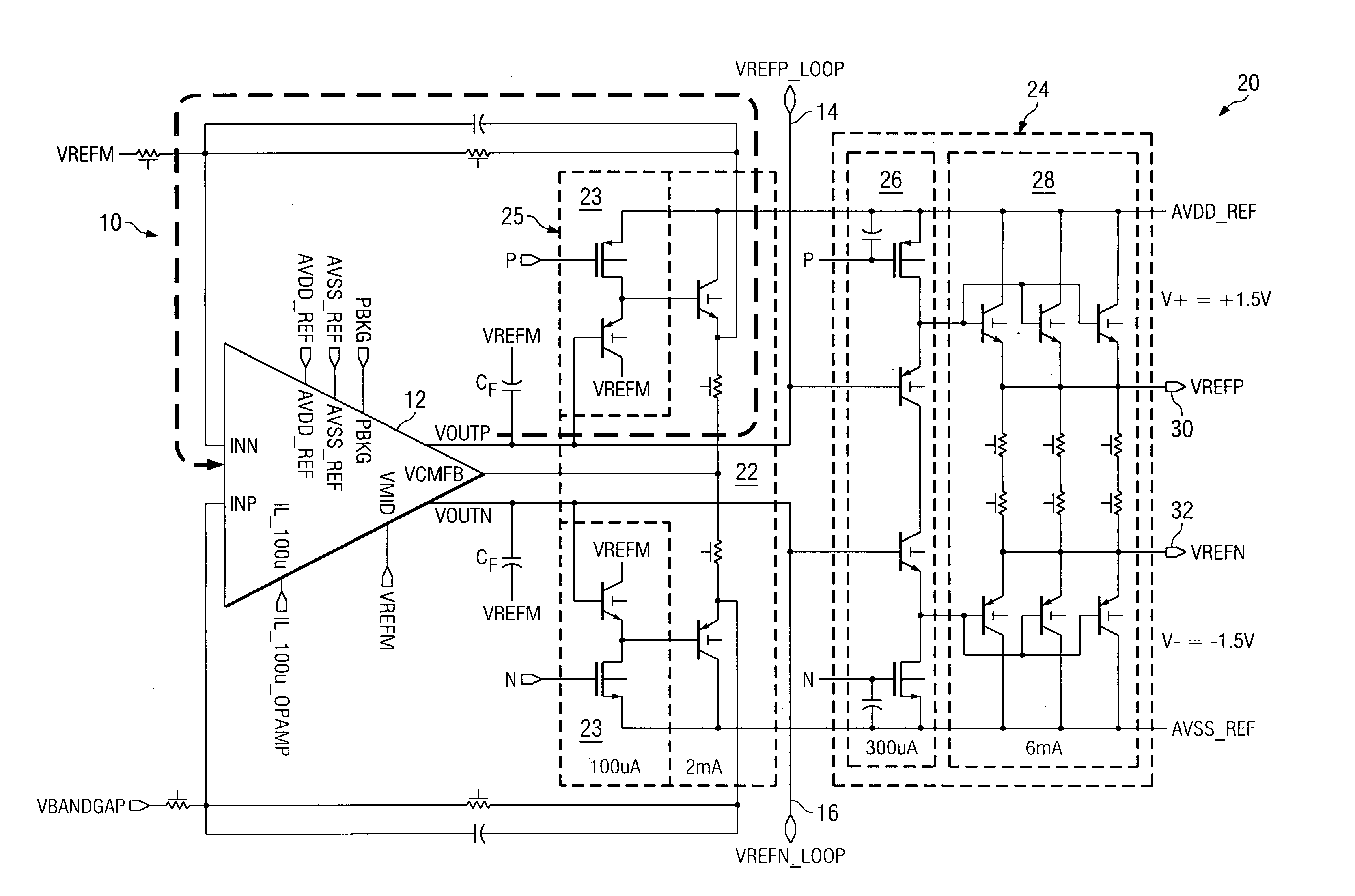
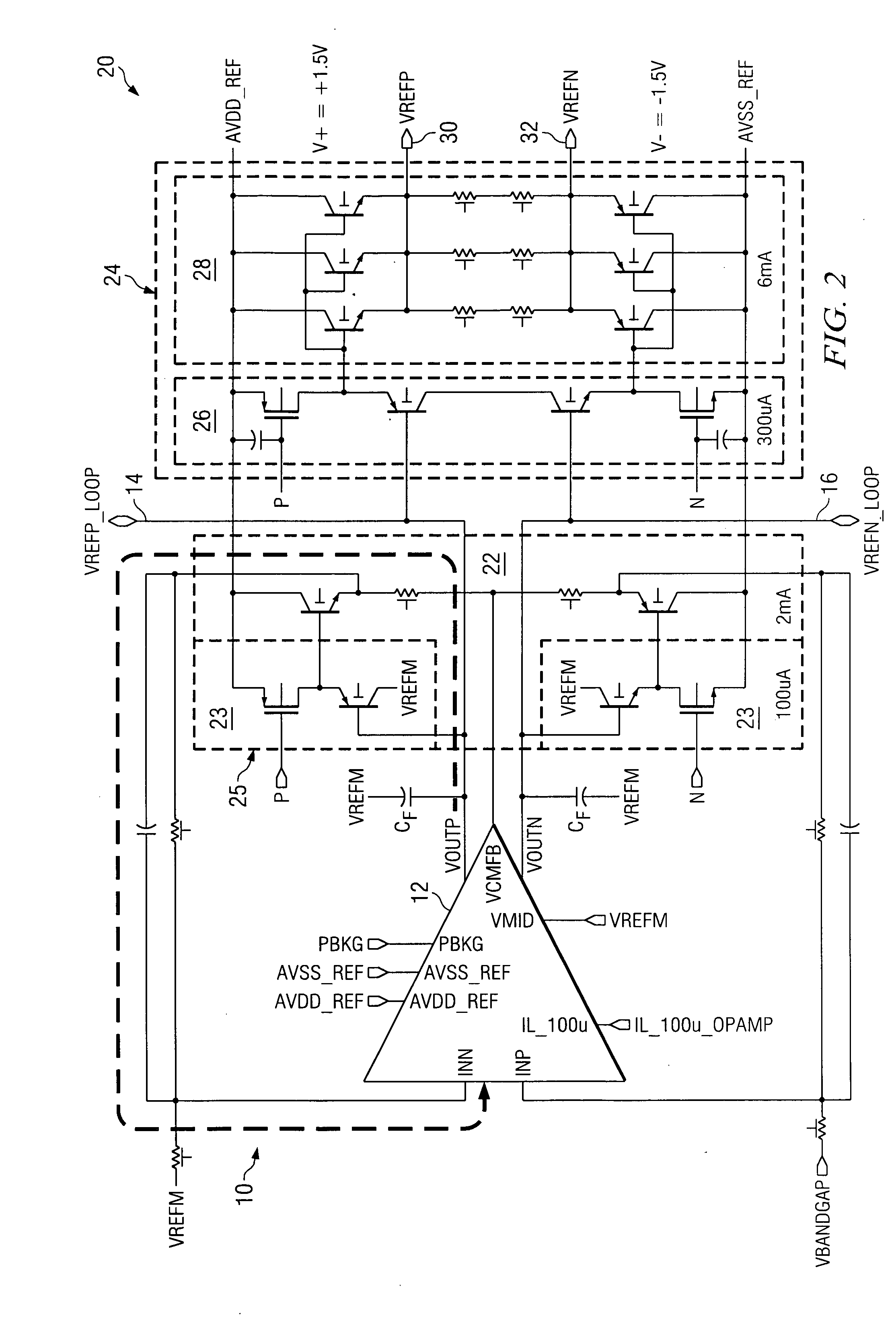
[0019] The present invention is targeted at low-impedance voltage reference circuits. In one embodiment of the invention shown at 20 in FIG. 2, an open-loop buffer 24 implemented with bipolar or CMOS devices is utilized, based on the most elementary emitter-follower (or source-follower) topology. More complicated buffer schemes can be effortlessly accommodated in the frame in another embodiment of the invention. The simplicity of the open-loop buffer / driver 24 of the voltage reference lines indeed ensures extreme speed to the settling. Notice how the current flowing in the two devices (NPN, PNP) of the buffer 24 are conveniently and advantageously shared in the case of a differential system, where two differential voltage levels are to be generated at outputs 30 and 32. This solution is indeed more general in scope, and can also be advantageously adopted for single-ended systems without loss of efficiency.
[0020] In order to force the output voltage of the whole driver 20 to the des...
PUM
 Abstract
Description
Claims
Application Information