Storage device, file storage device, and computer system

a storage device and file storage technology, applied in the field of storage devices and file storage devices, can solve problems such as inability to store data inside caches, and achieve the effects of improving the data transfer capability of ferroelectric memory, high speed, and high reliability of semiconductor memory

Inactive Publication Date: 2007-02-22
SONY CORP
View PDF4 Cites 14 Cited by
  • Summary
  • Abstract
  • Description
  • Claims
  • Application Information

AI Technical Summary

Benefits of technology

[0059] It is therefore desirable in the present invention to improve the data transfer capability of a ferroelectric memory and provide a high speed, high reliability semiconductor memory device, file storage device, and computer system using such a ferroelectric memory.

Problems solved by technology

However, irrespective of their being insufficient in terms of access performance, they do not have caches inside them for dealing with power interruption along with sudden removal.

Method used


Image

  • Storage device, file storage device, and computer system
  • Storage device, file storage device, and computer system
  • Storage device, file storage device, and computer system

Examples


first embodiment

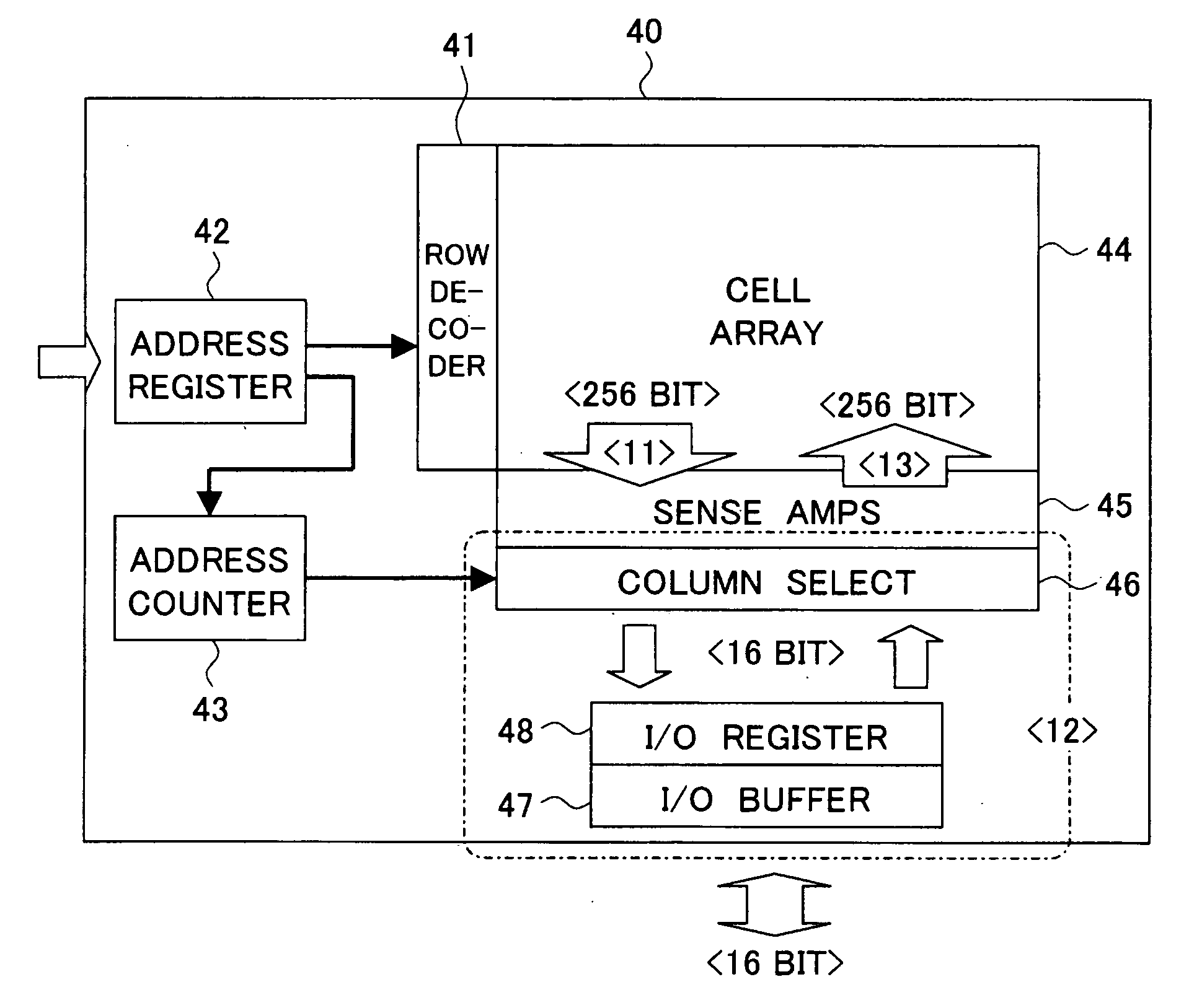
[0077]FIG. 5 is a block diagram showing a ferroelectric memory (semiconductor memory device) according to the present invention.

[0078] A ferroelectric memory chip 40 of FIG. 5 includes a row decoder 41, address register 42, address counter 43, memory cell array 44, sense amplifiers 45, column selector 46, input / output (I / O) buffer 47, and I / O register 48.

[0079] In the erroelectric memory chip 40, a mechanism of transferring continuous word data at a high speed is newly added to the ferroelectric memory of the related art.

[0080] Namely, in contrast to access routine of the ferroelectric memory of the already proposed related art of step where a word line and a plate line are selected from the row address, and the memory cell data is read out to the sense amplifiers, step where the sense amplifiers are selected from the column address and the data is input / output, and step where data is rewritten from the sense amplifiers into the memory cells, the present embodiment has the foll...

second embodiment

[0101]FIG. 7 is a block diagram showing a ferroelectric memory (semiconductor memory device) according to the present invention. FIG. 7 shows an example of introducing ECC error correction to an embodiment of the present invention. Here, high speed data transfer is executed while applying the error correction processing in units of 32 bits (2 words) at the time of the input / output of data.

[0102] A ferroelectric memory chip 40A of FIG. 7 includes a row decoder 41, address register 42, address counter 43A, memory cell array 44, sense amplifiers 45, column selector 46A, input / output (I / O) buffer 47, ECC decoder 50, ECC encoder 51, register 52, output register 53, input register 54, multiplexer (MUX) 55, and demultiplexer (DeMUX) 56 of FIG. 5.

[0103] In the present example as well, rather than the processing of basic access routine of step where a word line and a plate line are selected from the row address, and the memory cell data is read out to the sense amplifiers, step where the ...


PUM


Abstract

A storage device including a ferroelectric memory cell array including a plurality of memory cells; sense amplifiers connected to the bit lines and selected by a column address; an internal counter able to generate the column address; and a control part controlling data access, wherein the control part accesses data by a first processing of reading out a plurality of words of data from memory cells of a word line and a plate line selected according to a row address and storing it in the sense amplifiers, a second processing of selecting sense amplifiers from the column address and inputting/outputting data with the outside, and a third processing of writing back the data of the sense amplifiers into the memory cells, data being continuously input or output and transferred by repeatedly executing the second processsing using the column address generated in the internal counter for a group of words read out to the sense amplifiers at the first processing,and a file storage device and a computer system utilizing such a ferroelectric memory.

Description

CROSS REFERENCE TO RELATED APPLICATION [0001] The present invention contains subject matter related to Japanese Patent Application No. 2005-240057 filed in the Japan Patent Office on Aug. 22, 2005, the entire contents of which being incorporated herein by reference. BACKGROUND OF THE INVENTION [0002] 1. Field of the Invention [0003] The present invention relates to a storage device including a ferroelectric memory, a file storage device, and a computer system, more particularly relates to improvement of a data transfer capability of a ferroelectric memory and use of such a ferroelectric memory to realize a high speed, high reliability file storage device. [0004] 2. Description of the Related Art [0005] In recent years, a variety of semiconductor memories using new memory materials have been proposed. Many of these memories enable high speed random access irrespective of being novolatile. Application in the future as “next generation memories” is promising. [0006] As a representative...

Claims


Application Information

Patent Timeline
Patent Type & Authority Applications(United States)
IPC IPC(8): G11C11/22
CPCG11C11/22
Inventor NISHIHARA, TOSHIYUKINAKASHIMA, KATSUYATSUNEDA, YUKIHISA
Owner SONY CORP
Why Eureka
Try Eureka