Ternary alloy column grid array

a grid array and alloy technology, applied in the field of electronic components packaging, can solve the problems of mechanical reliability problems, thermal management issues,

Active Publication Date: 2007-02-22
ORACLE INT CORP
View PDF16 Cites 13 Cited by
  • Summary
  • Abstract
  • Description
  • Claims
  • Application Information

AI Technical Summary

Benefits of technology

[0008] In some embodiments lead-free alloy columns are joined to bonding pads on electronic packages having relatively low coefficients of thermal expansion (CTEs) using Pb-free solder from the same alloy system. In some embodiments Pb-free alloy columns are joined to bonding pads on printed circuit boards (PCBs) having relatively high CTEs using Pb-free solder from the same alloy system. In some embodiments the Pb-free columns soldered at one end to the low-CTE packages and at the other to the high-CTE boards accommodate the thermal expansion mismatch between the packages and boards while providing good electrical contact between the corresponding bonding pads.
[0011] In some embodiments, a thermal hierarchy in a Pb-free ternary alloy system is provided. In some embodiments a column is formed from an off-eutectic ternary alloy composition and is attached between an electronic package and a PCB using two distinct solders having off-eutectic compositions in the same ternary alloy system as the column, each solder with a distinct liquidus temperature, both of which are lower than the column liquidus temperature. In some embodiments, the first solder has a liquidus temperature more than 10° C. higher than a eutectic temperature in the ternary alloy system.

Problems solved by technology

Thermal management is also an issue in these systems.
Thermal expansion mismatch can cause mechanical reliability problems such as metal fatigue.

Method used


Image

  • Ternary alloy column grid array
  • Ternary alloy column grid array
  • Ternary alloy column grid array

Examples


example 1

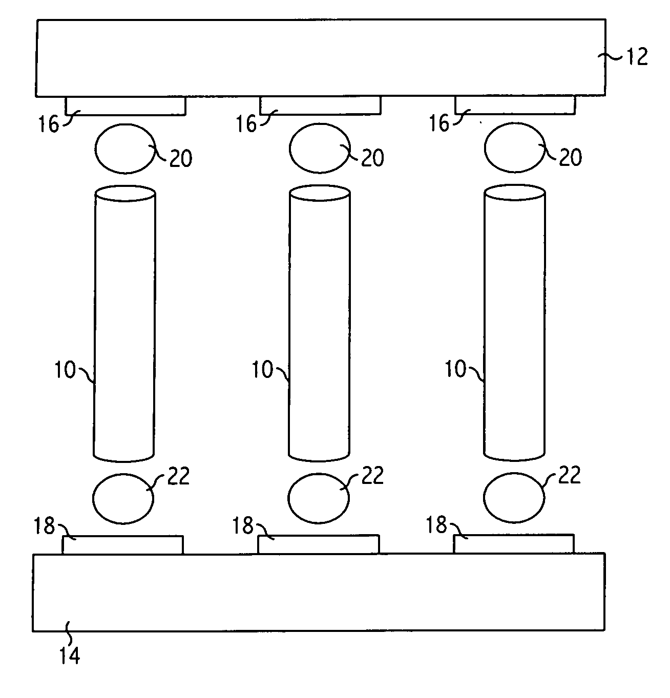
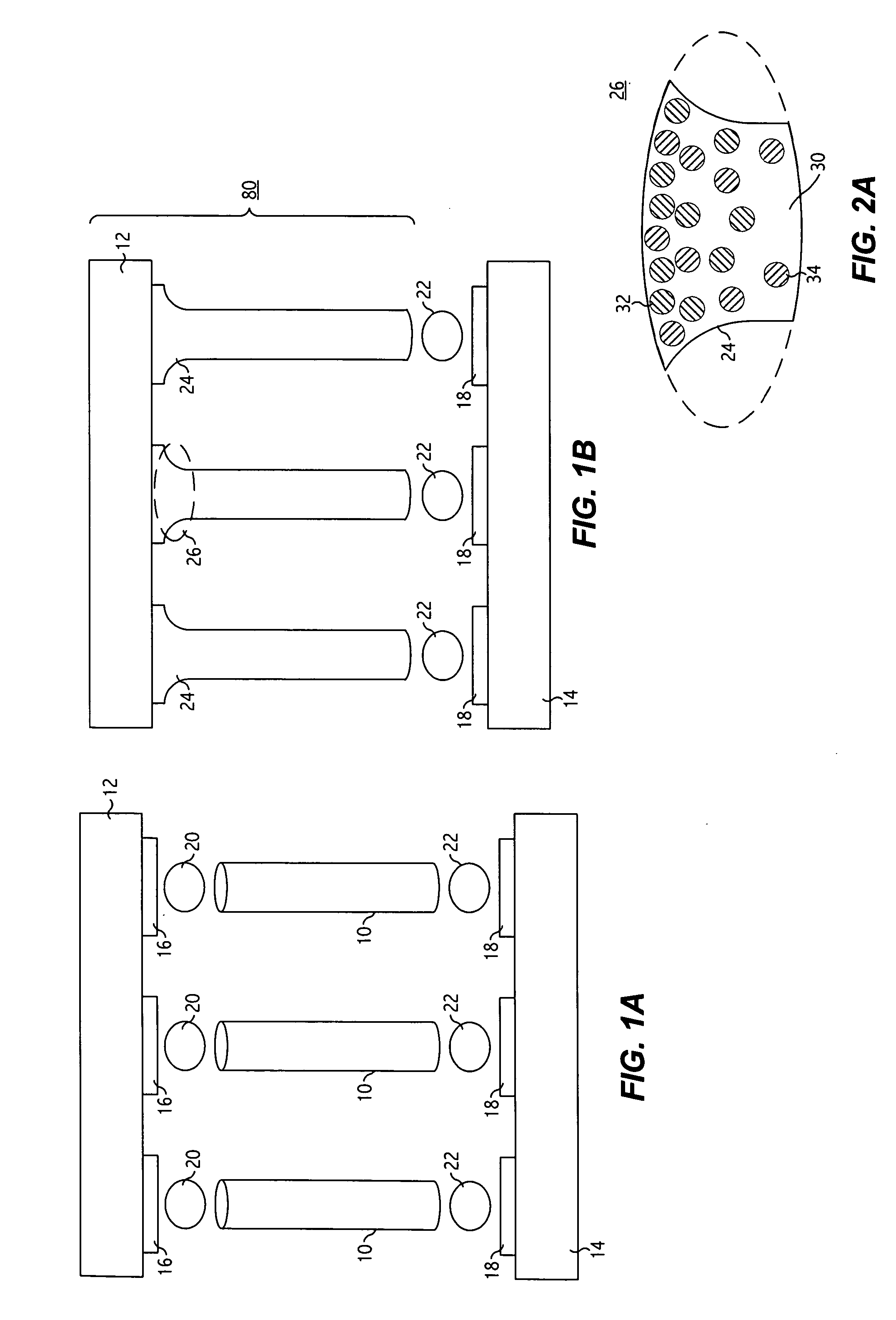
[0027]FIG. 1A depicts a chip carrier before attachment to a printed circuit board using an alloy column and two solder compositions comprising elements of a common ternary alloy system. In one preferred embodiment, a column 10 for attaching a chip carrier 12 to a printed circuit board (PCB) 14 is formed from approximately 80 percent by weight (80 w / o) tin and 20 w / o silver. This composition has a liquidus temperature of approximately 380-385° C. and a solidus temperature of approximately 230° C. The column 10 may be formed by any suitable method. For example, column 10 may be cast or cut from wire or ribbon, using any of the techniques standard in the solder industry. One end of the column is to be attached to the chip carrier 12 with a quantity of solder 20 and the other end to the PCB 14 with a quantity of solder 22. Generally both chip carriers and PCBs have solderable bonding pads 16, 18 for attaching one to the other and allowing for input and output operations. Often the bondi...

example 2

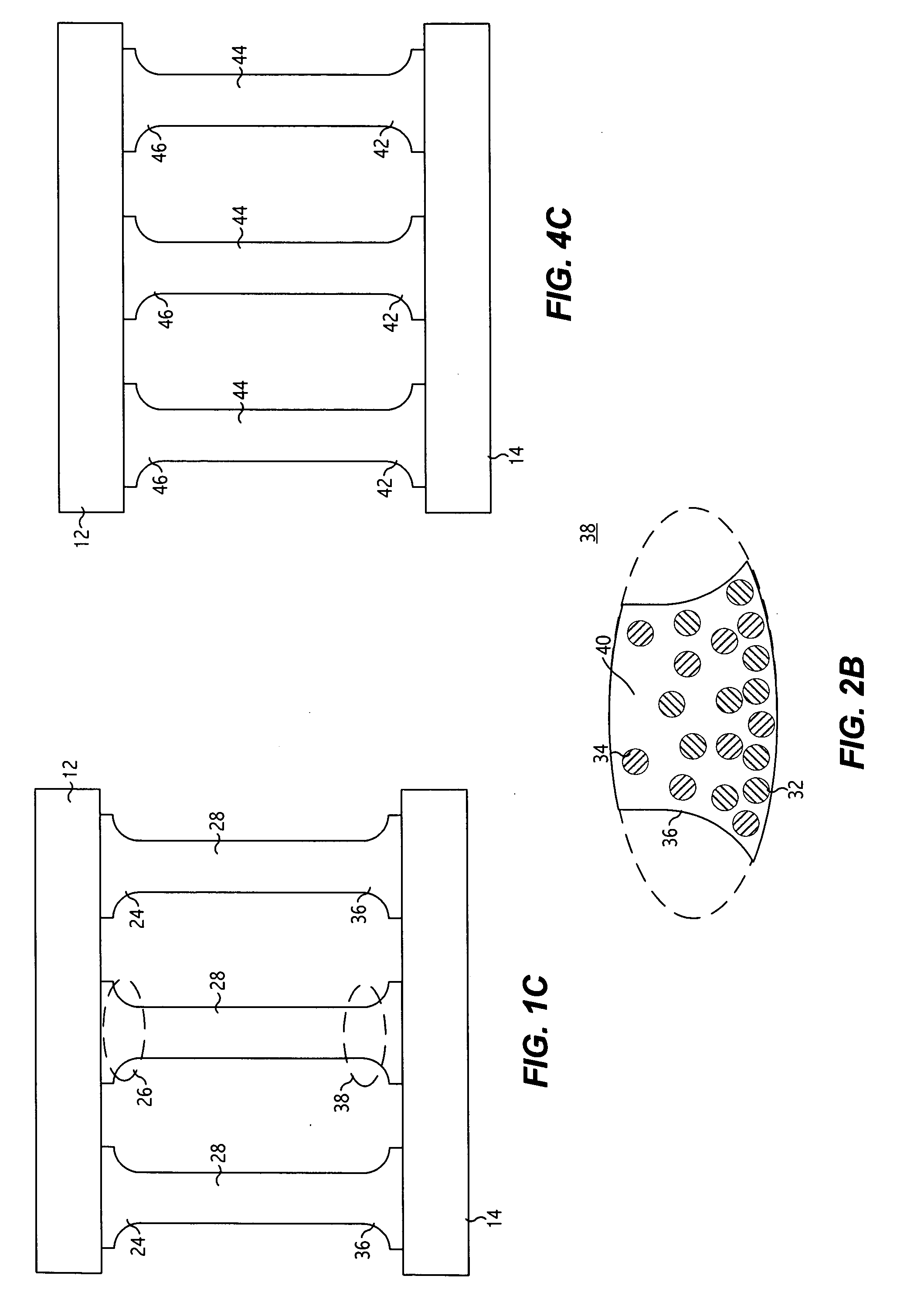
[0034]FIG. 4A depicts a chip carrier before attachment to a printed circuit board using an alloy column and two solder compositions comprising elements of a common ternary alloy system. The column 10 for attaching a chip carrier 12 to a printed circuit board (PCB) 14 is formed from an alloy of Ag in Sn with a composition higher in Ag than the Sn—Ag eutectic composition, having a liquidus temperature above about 300° C. Referring to FIG. 4B, one end of the alloy column 10 is attached to a bonding pad 18 on the PCB using a solder 20 with a composition significantly richer in both silver and copper than the SAC eutectic composition and having a liquidus temperature greater than approximately 240° C. and a solidus temperature of approximately 216° C., forming a high-temperature solder joint 42. To accomplish the attachment, the column 10 is aligned to a bonding pad 18, solder 20 is applied to the bonding pad 18, the column 10, or both, and the solder 20 is heated to a temperature above ...

example 3

[0036] Alloy columns may be prepared for use by attaching the relatively high liquidus solder to one end of the column. Referring to FIG. 5A, the solder 20 can be attached to the alloy column 10, producing a column preform 70, shown in FIG. 5B. As shown in FIG. 6, the preform 70 can then be placed so the solder makes contact with a substrate 72, such as a PCB or a chip carrier, and the solder can be flowed to attach the column to the substrate. Additional preforms 74 may optionally be attached during the same or a subsequent bonding operation. FIG. 7 depicts a preform 70 attached to a tape 76 for use in tape automated bonding. The tape 76 may support many additional preforms 74.


PUM

PropertyMeasurementUnit
eutectic temperatureaaaaaaaaaa
melting pointaaaaaaaaaa
liquidus temperatureaaaaaaaaaa

Abstract

Techniques and structures have been developed for providing lead-free column grid array interconnect structures. An exemplary interconnect has a body, a first joint, and a second joint, all having compositions off the eutectic composition in a ternary alloy system, the first joint having a ternary composition distinct from the body composition, and the second joint having a ternary composition distinct from the body composition and the first joint composition. The interconnect may be formed by solidifying a solder, having a Sn-poor ternary composition in the Sn—Ag—Cu alloy system, in contact with a column, having a Ag-rich Cu-deficient composition in the same system, and a bonding pad or bare substrate. A second solder, having a Sn-rich ternary composition, may be solidified in contact with the column and a second bonding pad or bare substrate. In some embodiments joints may be severed and reformed by remelting and resolidifying the lower-liquidus solder.

Description

CROSS-REFERENCE TO RELATED APPLICATION(S) [0001] This application claims the benefit under 35 U.S.C. § 119(e) of U.S. Provisional Application No. 60 / 708,837, filed Aug. 17, 2005, entitled “GRID ARRAY PACKAGE USING TIN / SILVER COLUMNS” by David G. Love and Bidyut Sen, which application is hereby incorporated by reference.BACKGROUND [0002] 1. Field of the Invention [0003] This invention relates to the packaging of electronic components using lead-free structures and materials. [0004] 2. Description of the Related Art [0005] In the electronics industry, it is often necessary to attach chip packages and bare die to printed circuit boards (PCBs). The attachment structures provide electrical connections as well as mechanical support. Thermal management is also an issue in these systems. Circuit boards are often constructed of organic materials with relatively high coefficients of thermal expansion (CTEs), while ceramic chip carriers have relatively low CTEs. Thermal expansion mismatch can ...

Claims


Application Information

Patent Timeline
Patent Type & Authority Applications(United States)
IPC IPC(8): B22F7/02B32B19/00H01L23/48
CPCH01L21/4853H01L23/49811H01L23/4985H01L23/49866H01L24/10H01L24/81H01L2224/8121H01L2224/81815H01L2924/01029H01L2924/01051H01L2924/01074H01L2924/01082H01L2924/01322H01L2924/01327H01L2924/14H05K3/3436H05K3/3463H05K2201/10992H05K2203/0415H01L2924/00013H01L2924/01006H01L2924/01024H01L2924/01033H01L2924/01047H01L2924/0105H01L2924/014H01L2224/13099Y10T428/12903Y10T428/12708Y10T428/12458Y10T428/12896Y10T428/12771Y10T428/12028Y02P70/613H01L2224/11334Y02P70/50
Inventor LOVE, DAVIDSEN, BIDYUT
Owner ORACLE INT CORP
Why Eureka
Try Eureka