
Method for providing a current sink model for an asic

a current sink and asic technology, applied in the field of providing a current sink model for an asic, can solve the problems of increasing the current delivered to the circuit (logic) elements, increasing the power consumption of complex chip designs, and increasing the complexity of application-specific integrated circuit (asic) designs, etc., to achieve the effect of simplifying calculations and simulations, and performing quickly and easily

Inactive Publication Date: 2007-02-22
AVAGO TECH WIRELESS IP SINGAPORE PTE
View PDF26 Cites 1 Cited by
  • Summary
  • Abstract
  • Description
  • Claims
  • Application Information

AI Technical Summary

Benefits of technology

[0012] In accordance with another aspect of the invention, the current sink model can be included in simulations for analyzing such chip design issues as the supply voltage droop that can be predicted or estimated to occur at one or more regions of interest on the chip. In accordance with an exemplary method for analyzing voltage droop, a region simulation circuit model is first created or otherwise provided. The region simulation circuit model comprises a number of tiled, substantially identical sub-region simulation circuit models, each representing the supply voltage (VDD) distribution network (i.e., the metal supply voltage lines or tracks) in one of a number of corresponding sub-regions of the region. The sub-region simulation circuit models are made identical or at least substantially identical to simplify the calculations and simulation, so that they can be performed quickly and easily at an early stage in the design process. Thus, in other words, there is a representative sub-region simulation circuit model that is tiled, i.e., repeated, over all or substantially all of the sub-regions in the region. This mosaic of sub-region simulation circuit models forms or defines the overall (region) simulation circuit model that can then be provided to an electronic simulator tool.

Problems solved by technology

As application-specific integrated circuit (ASIC) designs have become more complex, design issues associated with power distribution on the chip have become more important.
For example, the more complex chip designs consume more power than previous designs, which in turn increases the current delivered to the circuit (logic) elements.
Large transients may occur in the power supply network due to switching events and instantaneous changes in current.
A reduction in the supply voltage (VDD) due to the change in current is known as a “voltage droop.” Severe voltage droops can cause adverse circuit operation.
Voltage droop is typically worst at regions of the chip farthest from the solder bumps through which power is supplied to the chip through the chip packaging.
A simple, static model based upon such (likely inaccurate) assumptions will almost certainly be less accurate than a model based upon actual design parameters.
Nevertheless, as noted above, the conventional modeling method, involving running simulations through extracted R-C (resistance-capacitance) values and gates, cannot be performed early in the design process.
In addition, the method is relatively slow.
Other types of simulations similarly suffer from the shortcoming that they cannot readily be performed early in the ASIC design process because they rely in part upon completed artwork.
This method not only requires a completed logic design and artwork but also is relatively slow.

Method used


Image

  • Method for providing a current sink model for an asic
  • Method for providing a current sink model for an asic
  • Method for providing a current sink model for an asic

Examples


Embodiment Construction

[0033] In the following description, like reference numerals indicate like components to enhance the understanding of the invention through the description of the drawings. Also, although specific features, configurations, arrangements and steps are discussed below, it should be understood that such specificity is for illustrative purposes only. A person skilled in the relevant art will recognize that other features, configurations, arrangements and steps are useful without departing from the spirit and scope of the invention.

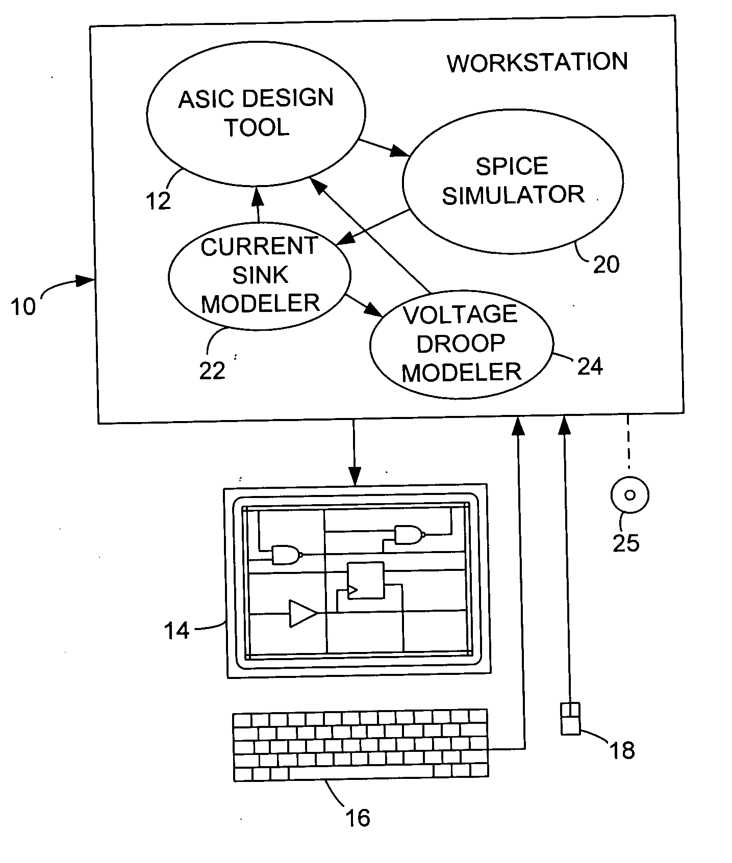
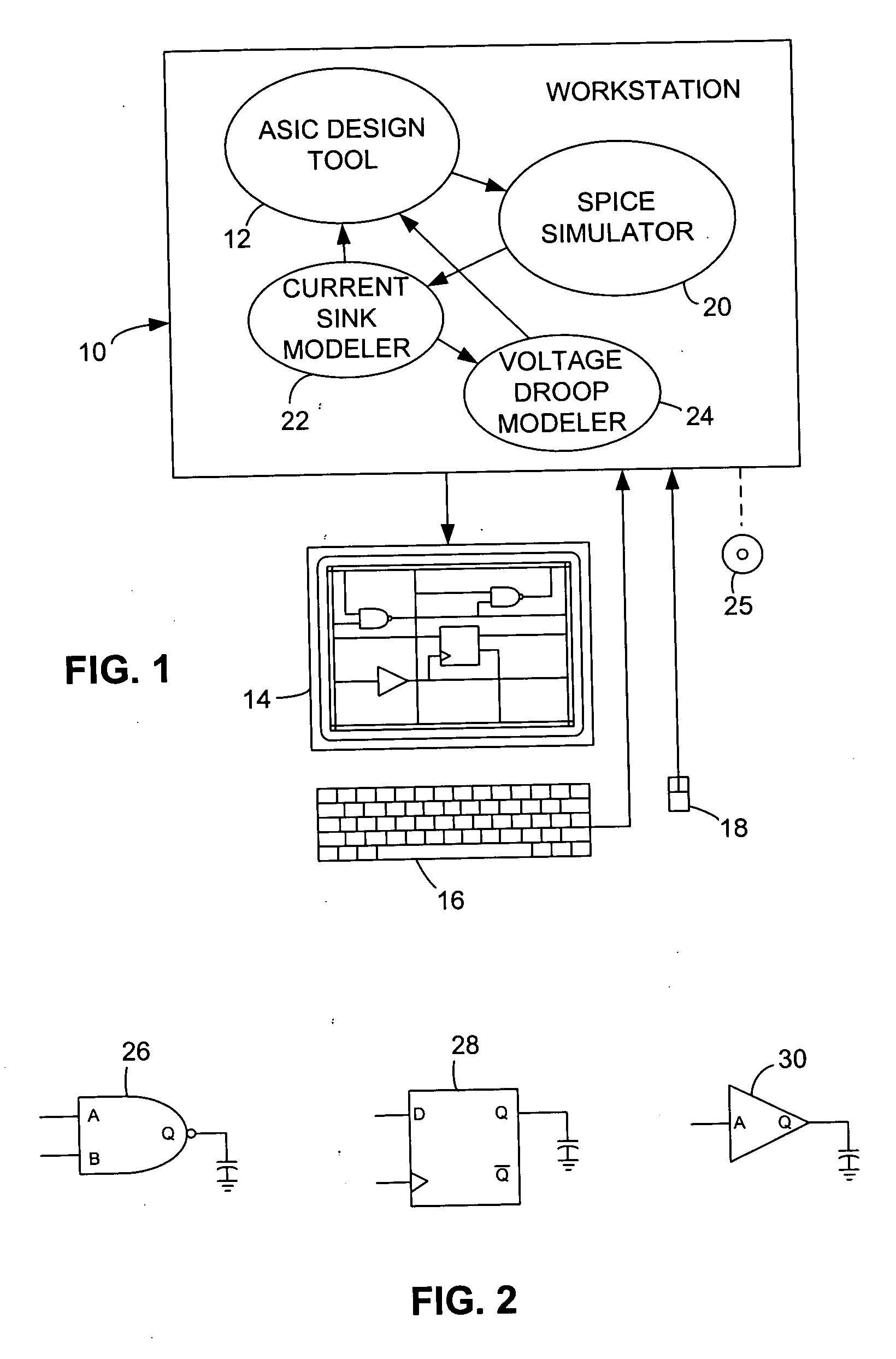
[0034] As illustrated in FIG. 1, an ASIC designer working on a conventional computer 10 can use various electronic design automation (EDA) software tools to design an ASIC, perform simulations, and perform other tasks relating to designing and producing an ASIC. For example, a conventional ASIC design tool 12 or tool set can be used to build a circuit model by selecting and interconnecting gates and other circuit elements, placing the elements in the desired p...


PUM


Abstract

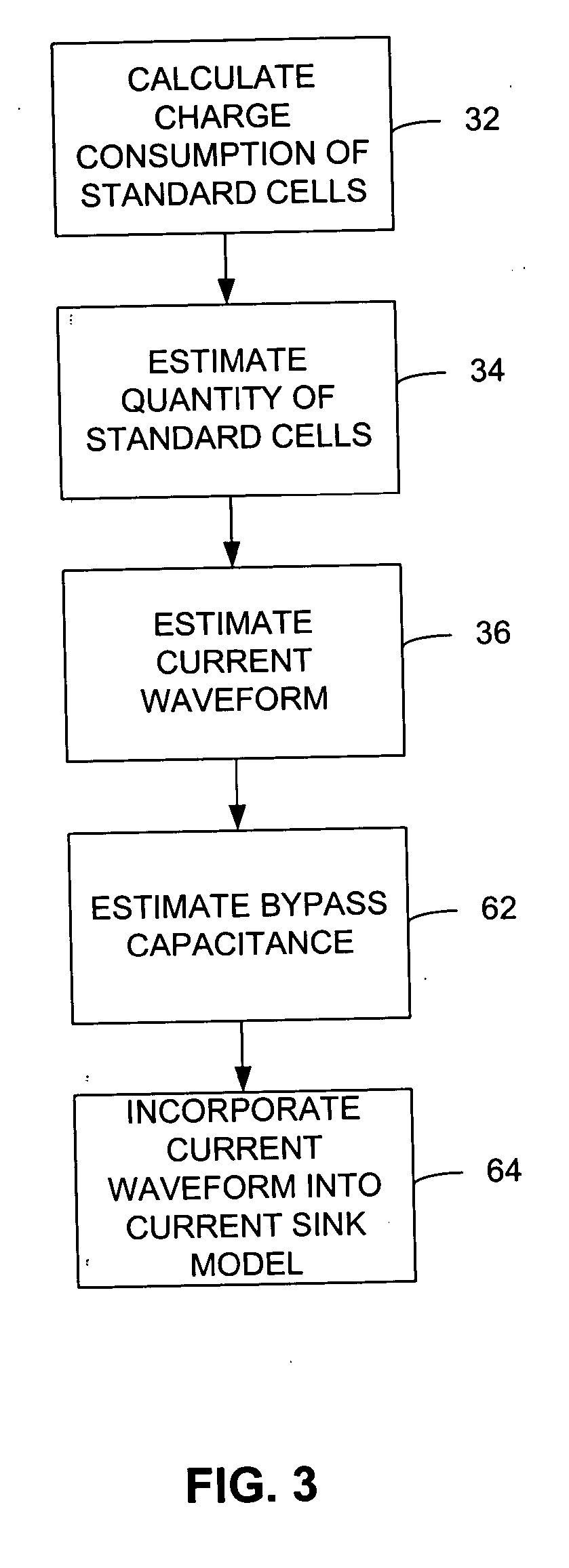
A current sink model is provided by determining the charge consumed by each type of a predetermined group of standard cell types under each of a plurality of conditions, determining the quantity of such standard cells of each type in the region of interest on the chip, and then using the charge consumption and quantity of standard cells of each type to create a waveform representing current over time.

Description

DESCRIPTION OF THE RELATED ART [0001] As application-specific integrated circuit (ASIC) designs have become more complex, design issues associated with power distribution on the chip have become more important. For example, the more complex chip designs consume more power than previous designs, which in turn increases the current delivered to the circuit (logic) elements. Large transients may occur in the power supply network due to switching events and instantaneous changes in current. A reduction in the supply voltage (VDD) due to the change in current is known as a “voltage droop.” Severe voltage droops can cause adverse circuit operation. Voltage droop is typically worst at regions of the chip farthest from the solder bumps through which power is supplied to the chip through the chip packaging. [0002] Designing an ASIC (or, for that matter, any other type of integrated circuit chip) involves a number of steps. Early in the process, functional specifications and performance requi...

Claims


Application Information

Patent Timeline
Patent Type & Authority Applications(United States)
IPC IPC(8): G06F17/50
CPCG06F17/5022G06F30/33
Inventor FAOUR, FOUAD A.STONG, GAYVIN E.
Owner AVAGO TECH WIRELESS IP SINGAPORE PTE
Learn More