Semiconductor storage device

a technology of semiconductor devices and storage devices, applied in semiconductor devices, solid-state devices, instruments, etc., can solve the problems of increasing chip area, increasing product cost, and and achieve the effect of complicating the manufacturing process and raising product cos

Active Publication Date: 2007-03-01
RENESAS ELECTRONICS CORP
View PDF6 Cites 5 Cited by
  • Summary
  • Abstract
  • Description
  • Claims
  • Application Information

AI Technical Summary

Benefits of technology

[0010] However, when the third diffusion region 221 (FIG. 39) is present, as in Related Art Example 2, a step of forming the third diffusion region 221 becomes necessary. This complicates the manufacturing process and may raise product cost.

Problems solved by technology

This complicates the manufacturing process and may raise product cost.
This may lead to an increase in chip area.
However, if the third diffusion region 221 and a sense amplifier SA are connected, read-out can no longer be performed for every cell that is to be read out.
As a result, if the third diffusion region 221 becomes a common power supply, there is the danger of a decline in speed at read-out of the cell.

Method used


Image

  • Semiconductor storage device
  • Semiconductor storage device
  • Semiconductor storage device

Examples


first embodiment

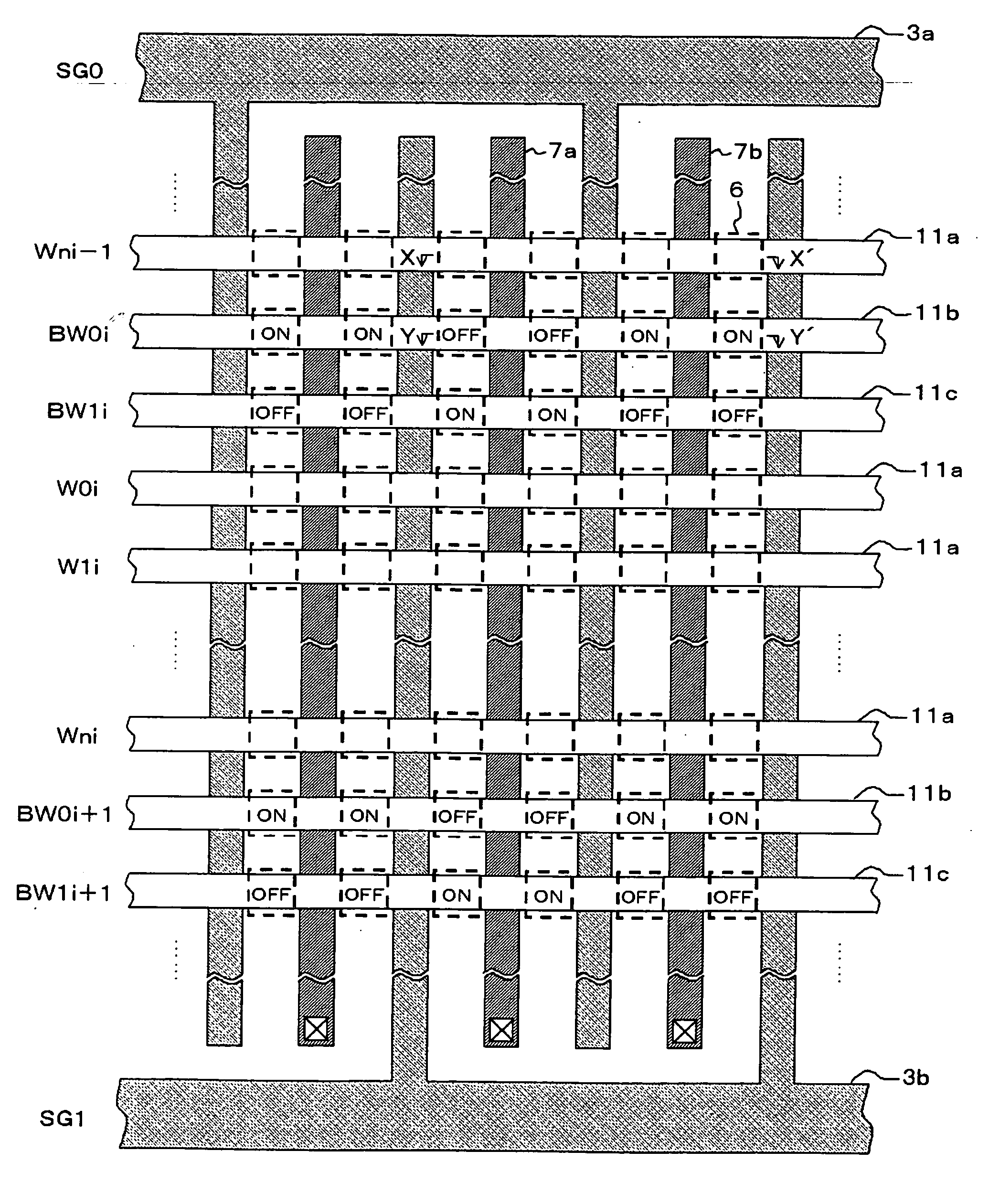
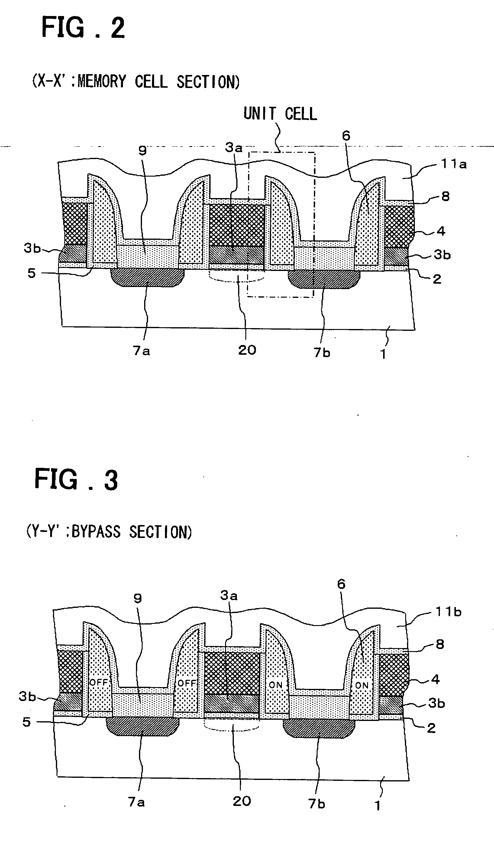
[0072]FIG. 1 is a partial plan view schematically illustrating the structure of a semiconductor storage device according to a first embodiment of the present invention, FIG. 2 is a partial sectional view taken along line X-X′ of FIG. 1 schematically illustrating the structure of the semiconductor storage device according to the first embodiment, and FIG. 3 is a partial sectional view taken along line Y-Y′ of FIG. 1 schematically illustrating the structure of the semiconductor storage device according to the first embodiment.

[0073] The semiconductor storage device according to the first embodiment is a non-volatile semiconductor storage device that stores 2-bit information per cell. The semiconductor storage device includes a substrate 1, an insulating film 2, a first select gate 3a, a second select gate 3b, an insulating film 4, an insulating film 5, a floating gate 6, a first diffusion region 7a, a second diffusion region 7b, an insulating film 8, an insulating film 9, a first con...

second embodiment

[0142] A semiconductor storage device according to a second embodiment of the present invention will now be described with reference to the drawings. FIG. 23 is a partial sectional view schematically illustrating the structure of a semiconductor storage device according to a second embodiment of the present invention, and FIGS. 24A to 26I are process sectional views useful in describing a method of manufacturing the semiconductor storage device according to the second embodiment.

[0143] The semiconductor storage device according to the second embodiment differs in terms of the structure of an ON cell [a floating gate 6 in the ON state (erase state) among the floating gates 6 underlying the second control gate 11b and third control gate 11c in FIG. 1] in the bypass section of the semiconductor storage device according to the first embodiment. In the semiconductor storage device according to the second embodiment, as shown in FIG. 23, the second control gate 11b and floating gate 6 ar...

third embodiment

[0155] A semiconductor storage device according to a third embodiment of the present invention will now be described with reference to the drawings. FIG. 27 is a partial sectional view schematically illustrating the structure of a semiconductor storage device according to a third embodiment of the present invention, and FIGS. 28A to 28C are process sectional views useful in describing a method of manufacturing the semiconductor storage device according to the third embodiment.

[0156] The semiconductor storage device according to the third embodiment differs in terms of the structure of an ON cell [a floating gate 6 in the ON state (erase state) among the floating gates 6 underlying the second control gate 11b and third control gate 11c in FIG. 1] in the bypass section of the semiconductor storage device according to the first embodiment. In the semiconductor storage device according to the third embodiment, as shown in FIG. 27, the structure is such that the floating gate underlying...


PUM


Abstract

A semiconductor storage device in which product cost is reduced includes a memory cell section (cells belonging to word lines) and a bypass section (cells belonging to bypass word lines). The memory cell section has a select gate, floating gates, a first diffusion region, a second diffusion region and a first control gate. The bypass section has the first select gate, the first diffusion region, the second diffusion region and a second control gate. The second control gate controls a channel in an area between the select gate and the first diffusion region or between the select gate and the second diffusion region. The channel of the bypass section becomes a current supply path when a cell of the memory cell section is read out.

Description

FIELD OF THE INVENTION [0001] This invention relates to a semiconductor storage device having cell transistors and, more particularly, to a semiconductor storage device for storing multiple-bit information per cell. BACKGROUND OF THE INVENTION [0002] In a semiconductor storage device according to the prior art, a non-volatile semiconductor storage device having a cell transistor shown in FIG. 38 is known as a non-volatile semiconductor storage device that stores multiple-bit information per cell (Related Art Example 1). The non-volatile semiconductor storage device according to Related Art Example 1 includes: two band-like regions 123a, 123b formed in a surface layer of a semiconductor substrate 121 so as to embrace a band-like semiconductor layer 124a of a first conductivity type, the regions 123a, 123b being of the opposite conductivity type; a first floating gate 127a formed from the one region 123a of the opposite conductivity type to one side face of the semiconductor layer 124...

Claims


Application Information

Patent Timeline
Patent Type & Authority Applications(United States)
IPC IPC(8): H01L29/788
CPCG11C16/0491H01L27/115H01L29/7885H01L29/42324H01L27/11521H10B69/00H10B41/30
Inventor SUDO, NAOAKIKANAMORI, KOHJISANADA, KAZUHIKO
Owner RENESAS ELECTRONICS CORP
Why Eureka
Try Eureka