Image pickup device and image pickup system
- Summary
- Abstract
- Description
- Claims
- Application Information
AI Technical Summary
Benefits of technology
Problems solved by technology
Method used
Image

Examples
fourth embodiment
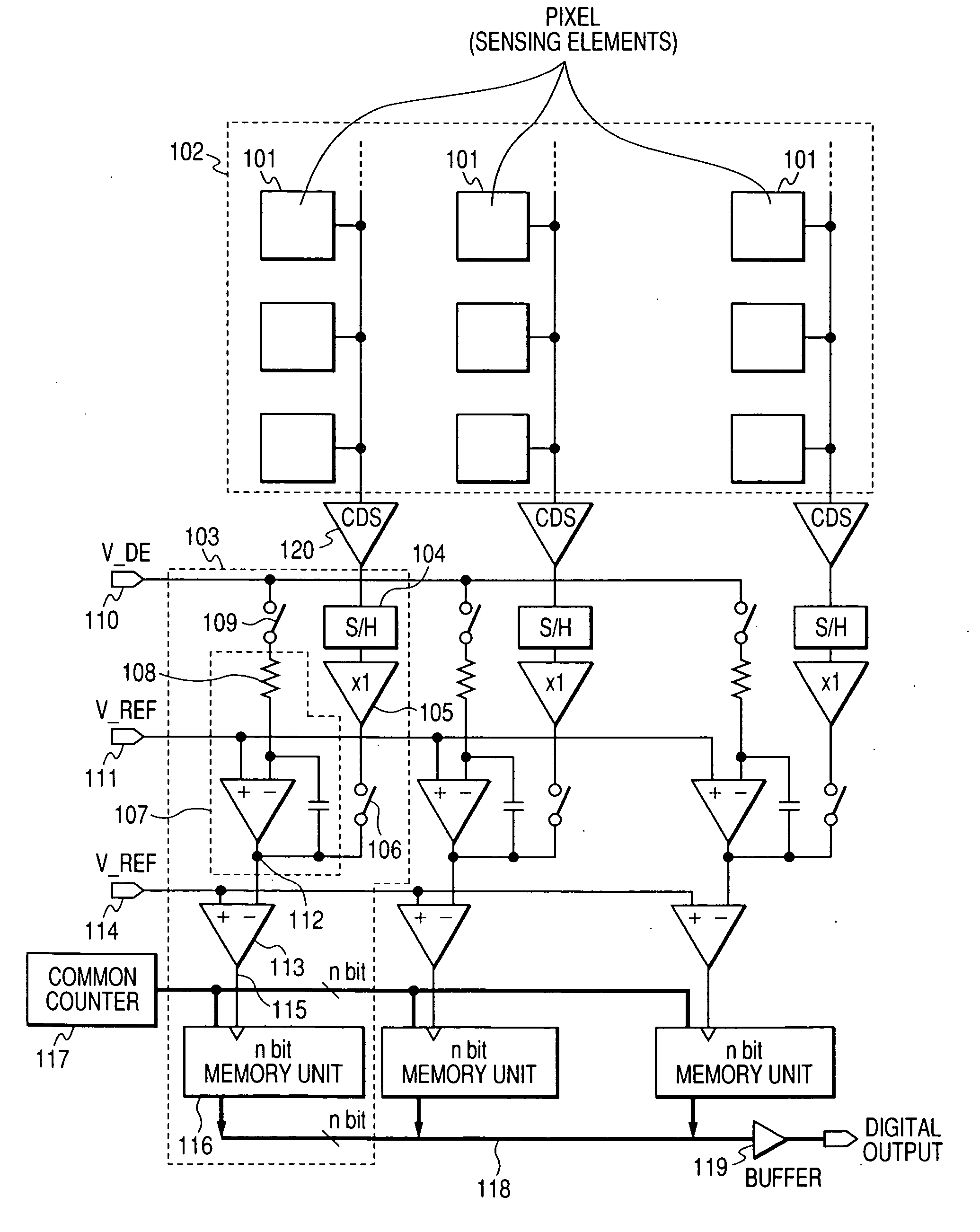
[0125]FIG. 10 shows a fourth embodiment of the present invention. In this and all subsequent embodiments, switches, operational amplifiers etc. will be shown in their modelized forms, unless otherwise required. In addition, switches and other devices necessary for peripheral operation are also omitted unless otherwise required. It is needless to say that the embodiments are by no means limited to the examples described below.
[0126] An object of the fourth embodiment is to substantially reduce the number of comparison steps required for an A / D conversion of N bits from 2 to the Nth power times. Another object is to shorten the time per step and significantly increase comparison speed by eliminating the need to apply an analog triangular wave, as was the convention, and adopting a method wherein a fixed voltage is supplied to all A / D converters. Yet another object is to achieve substantial simplification of the circuit size by using a method that eliminates the need for exclusive DAC...
fifth embodiment
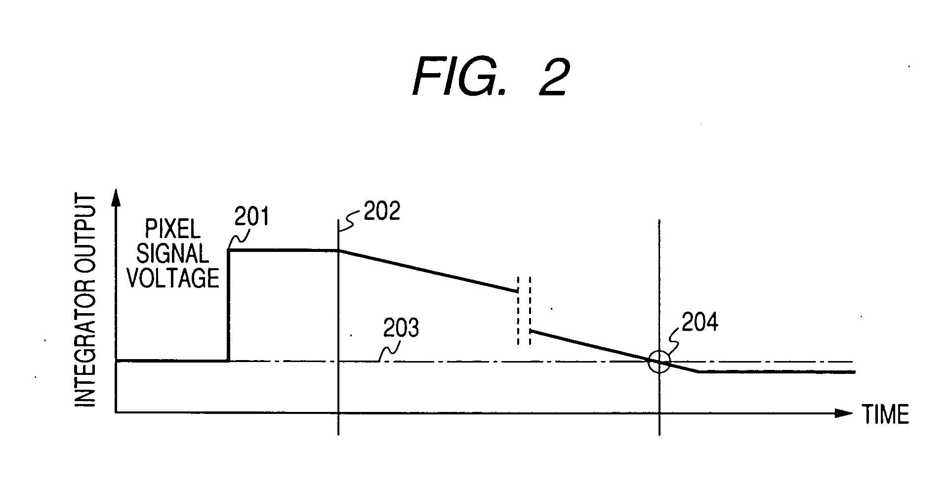
[0150]FIG. 15 is a diagram showing a fifth embodiment of the present invention. While the fourth embodiment involved directly writing the value of the pixel signal to the output of the integrator, the present embodiment also integrates the pixel signal.
[0151] An output from pixel 1501 is removed of its reset level at a CDS circuit 1502, maintained at sample holding (S / H) circuit 1503, and input to an integrator via a buffer 1504 and a switch 1505. At switch 1505, the input of the integrator can be switched from a signal from the pixel or a fixed voltage for integration 1506.
[0152] Also, with switch 1507, the fixed voltage for integration can be set to two fixed voltages V_DE1 (1508) and V_DE2 (1509). Reference numeral 1510 denotes an output portion of the integrator. A counter 1511 is connected to a memory unit 1512 for retaining high bits (n bits), and a memory unit 1513 for retaining low bits (m bits), and the memory units latch the counter value after receiving a trigger from a...
sixth embodiment
[0159]FIG. 17 shows a sixth embodiment of the present invention. With the exception of a switched capacitor 1701, the configuration is the same as in FIG. 10. Integrator operation is realized by operating the switched capacitor 1701 as a resistor that is equivalent to a resistor, while switching the switch 1702.
[0160] The operation as a line and a two-dimensional sensor when using this circuit is pursuant to the fourth embodiment. The advantage gained over the fourth embodiment is that while the RC time constant of an integrator will assume a fixed value when using a resistor, various resistance values can be achieved when using a switching capacitor by switching the frequency of the switch. This makes it possible to switch operations in response to various uses.
PUM
 Abstract
Description
Claims
Application Information