

Method for forming wiring on insulating resin layer
a technology of resin layer and wiring, which is applied in the direction of synthetic resin layered products, etching metal masks, paper/cardboard containers, etc., can solve the problems of insufficient joining strength between resin and wiring, difficult to roughen resin surface, and difficult to roughen resin prereg materials, etc., to achieve high joining strength
- Summary
- Abstract
- Description
- Claims
- Application Information
AI Technical Summary
Benefits of technology
Problems solved by technology
Method used
Image

Examples
example
[0050] A peel strength was tested on the wiring formed by the embodiment of the invention and comparison was made with the wiring formed by the related art method. The peeling test using a test piece according to “JIS Z2201”, and a tensile test method according to “JIS Z2241” are performed.
[0051] [Test Sample]
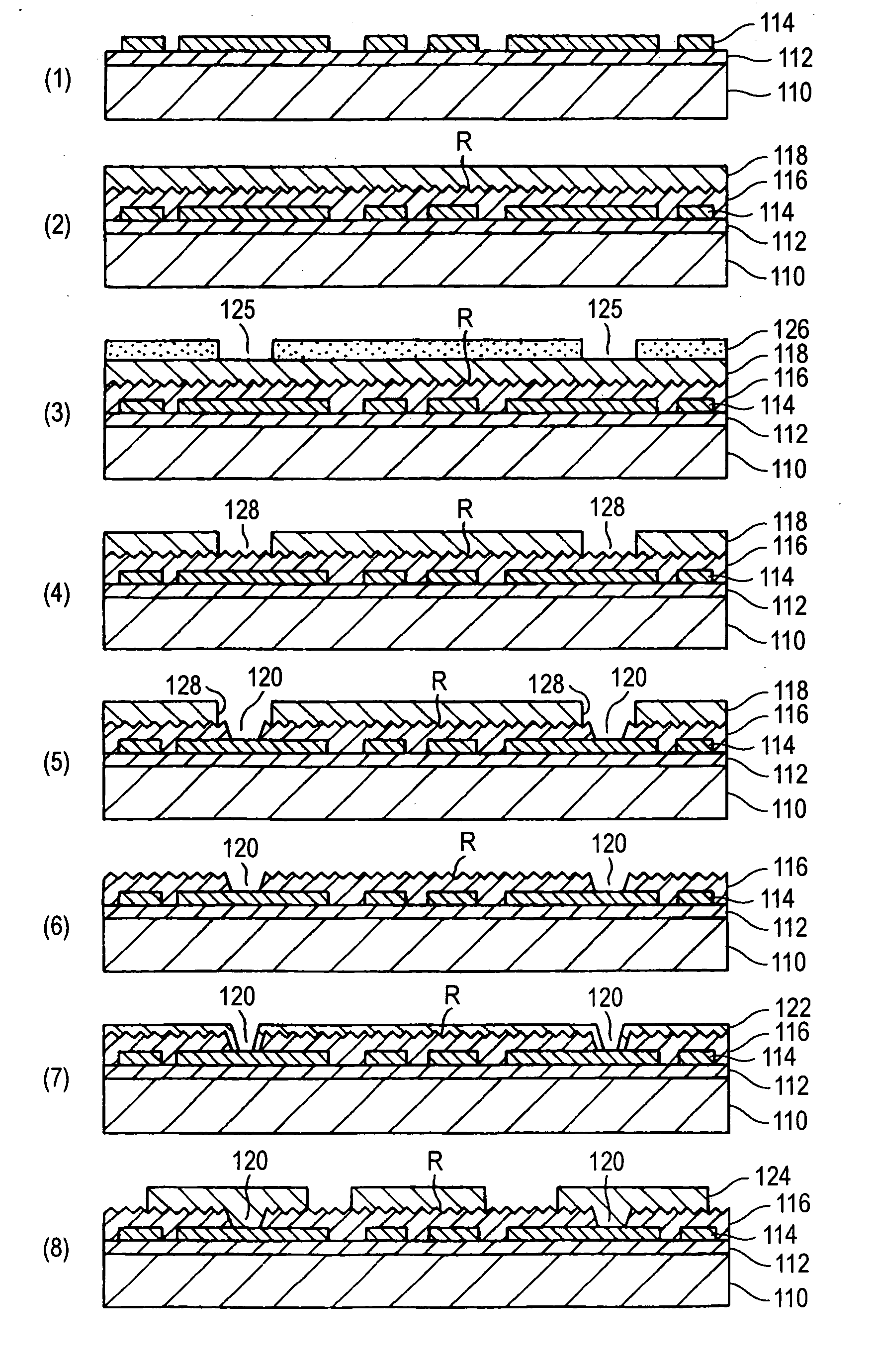
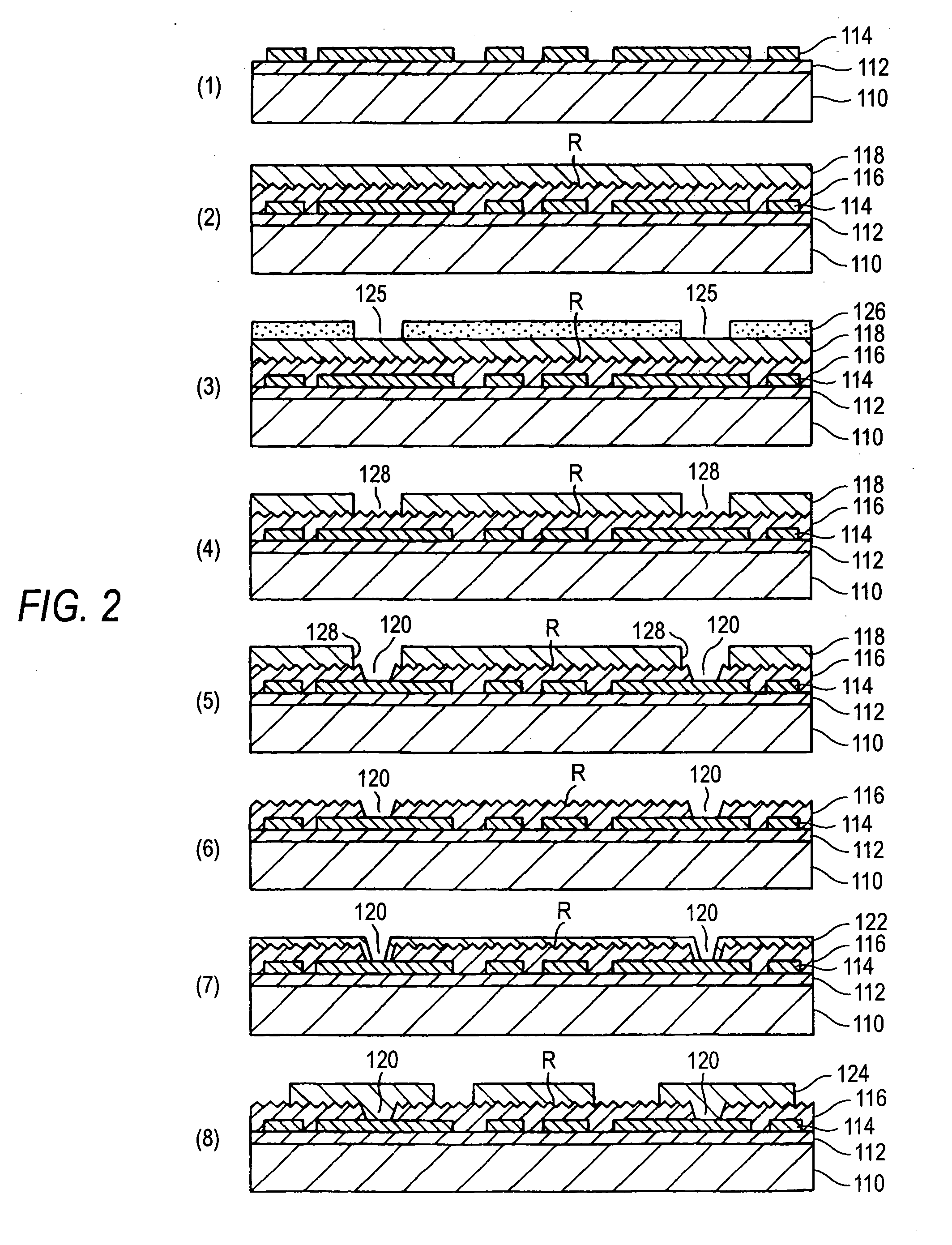
[0052] A sample in the same state as FIG. 2-(8) was prepared. However, the via hole 120 was not formed. The wiring 124 had a rectangular shape of 5 to 10 mm in width instead of an actual wiring pattern. The film thickness was 15 to 25 micrometers.
[0053] [Test Method]
[0054] A tensile test instrument was used to pull the rectangular wiring 124 (including the electroless-plated seed layer 122) in a longitudinal direction of the sample. On that occasion, the wiring was moved at a speed of about 30 mm / min while being raised vertically, and a tensile strength value was measured every five seconds. The average of these measurements is assumed as the peel strength of the insulating r...
PUM
 Abstract
Description
Claims
Application Information