

Trench semiconductor device of improved voltage strength, and method of fabrication
a semiconductor device and trench technology, applied in the field of trench semiconductor devices of improved voltage strength and method of fabrication, can solve the problems of undesired impurity diffusion from one part, unnecessarily wide deep guard rings, failure in field concentration mitigation, etc., and achieve the effect of improving the voltage-withstanding capability of trench semiconductor devices
- Summary
- Abstract
- Description
- Claims
- Application Information
AI Technical Summary
Benefits of technology
Problems solved by technology
Method used
Image

Examples
embodiment
of FIG. 7
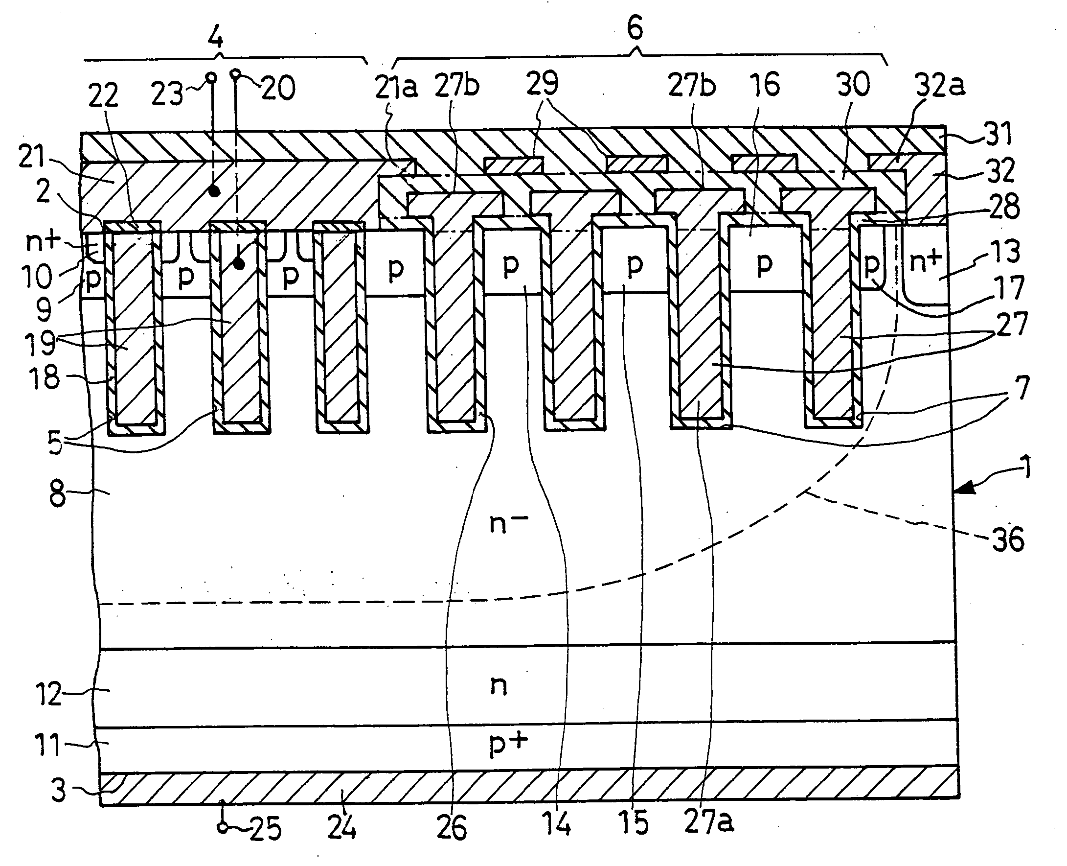
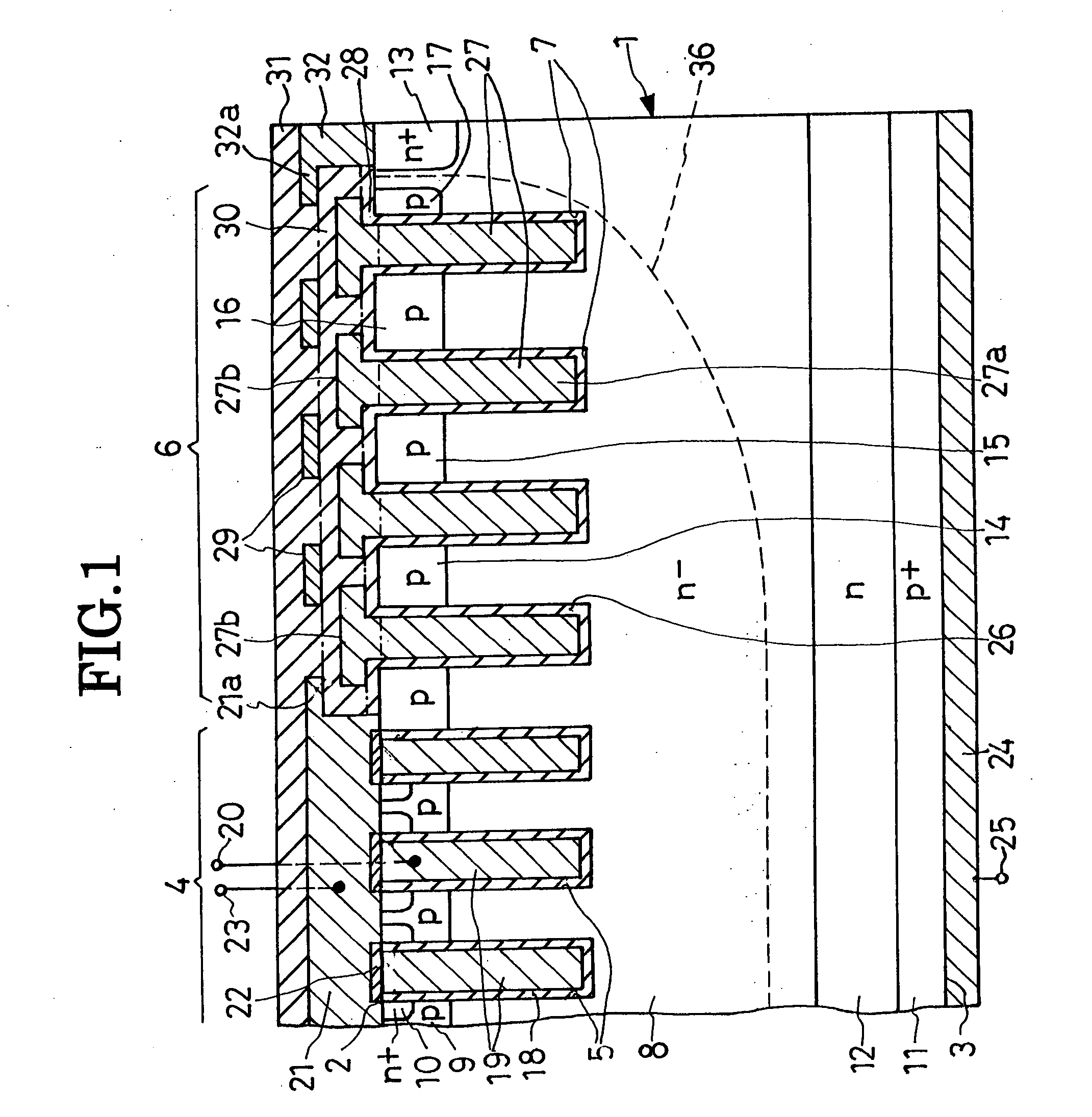
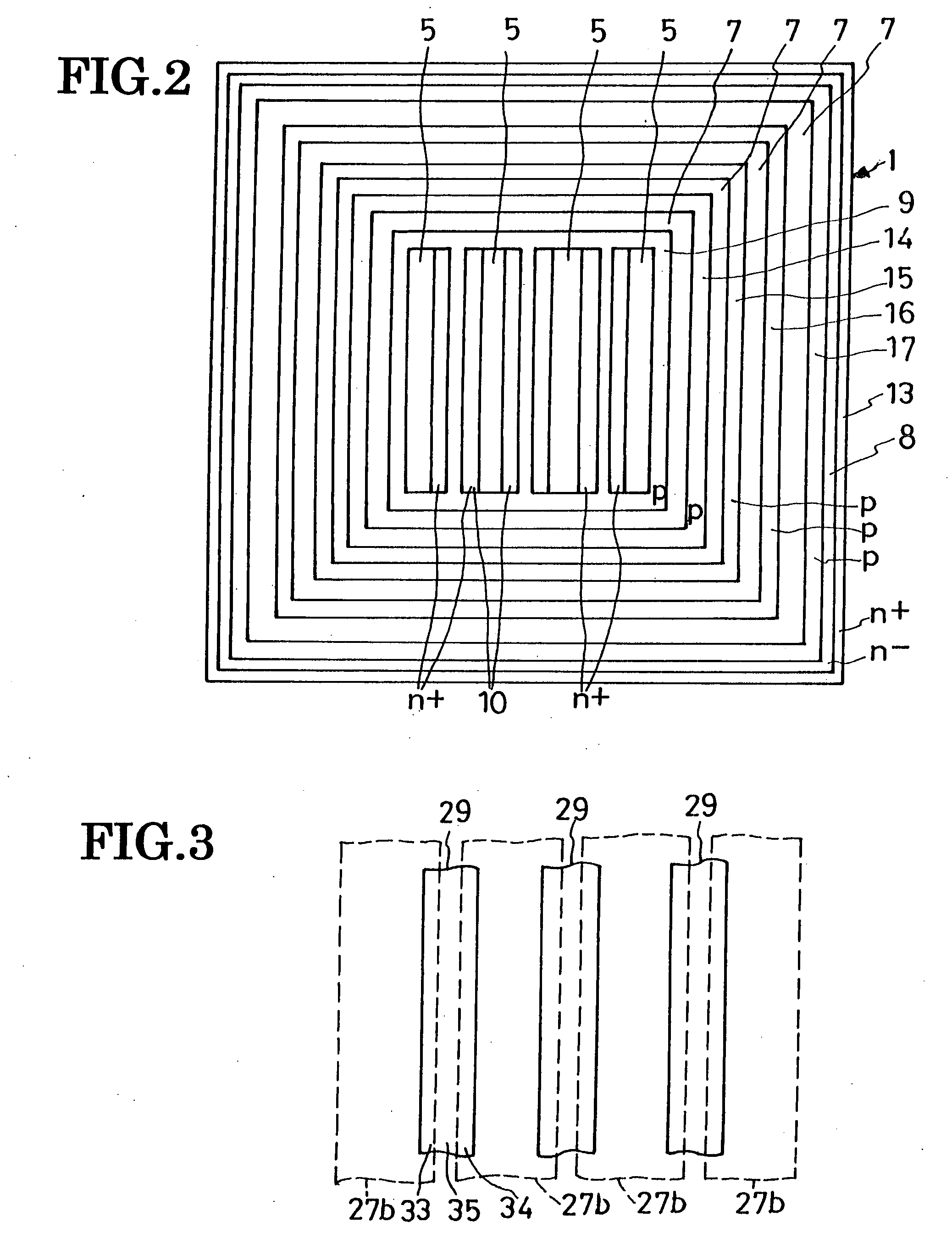
[0082] The IGBT shown here features modified cell trenches 5a, modified p-type base region 9a, and modified n+-type emitter regions 10a and is otherwise similar in construction to that of FIGS. 1-6. The cell trenches 5a are formed centrally in the semiconductor substrate 1 in latticelike arrangement, bounding islandlike n+-type emitter regions 10a in an array. The p-type base region 9a is exposed in part centrally in each emitter region 10a and in part between the latticed cell trenches 5a and the inmost annular guard trench 7.
[0083] It is understood that the cell trenches 5a receive cell trench conductors via cell trench insulators, and the guard trenches 7 receive the guard trench conductors via the guard trench insulators. Thus the second preferred form of IGBT offers the same benefits as the first.
Embodiment of FIG. 8
[0084] Another preferred form of IGBT according to the invention has a latticelike p-type base region 9b defining an array of islandlike n+-type emitter ...
PUM
 Abstract
Description
Claims
Application Information