Semiconductor device and automotive AC generator

a technology of semiconductor devices and ac generators, applied in the direction of manufacturing tools, cooking vessels, and so on, can solve the problems of inability to suppress interface reactions, low bond reliability, and insatiable suppression of interfacial reactions, so as to suppress interfacial reactions, reduce bond reliability, and suppress interfacial reactions high

Inactive Publication Date: 2007-03-15
HITACHI LTD
View PDF10 Cites 18 Cited by
  • Summary
  • Abstract
  • Description
  • Claims
  • Application Information

AI Technical Summary

Benefits of technology

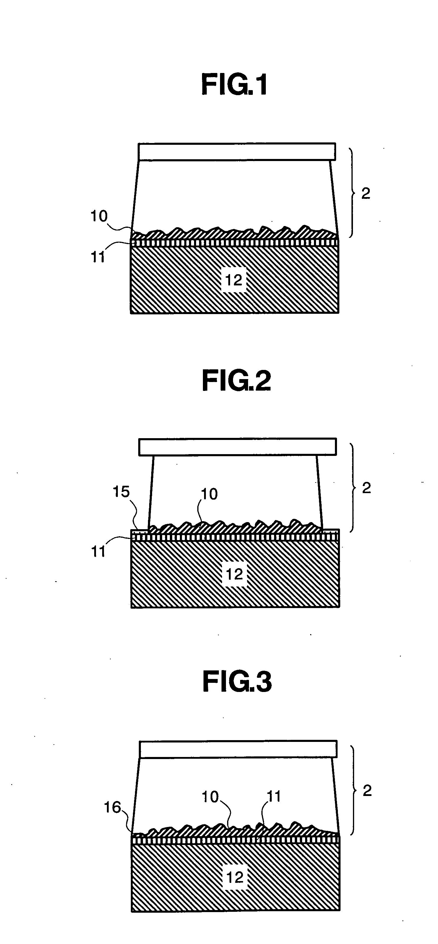
[0009] The method disclosed in patent document 2 using the Sn solder containing Ni is expected to suppress an interfacial reaction to some extent. However, an interfacial reaction occurs at high temperatures not lower than 200° C. because Cu6Sn5 and Cu3Sn are always in contact with the Cu and the Sn solder. Consequently, grains of a Cu—Sn compound grow continuously, voids are formed in the interface and the bond reliability is reduced.
[0011] Accordingly, it is an object of the present invention to provide a semiconductor device fabricated by using a low-cost bonding material for bonding a semiconductor device to a circuit, imparting low load to the environment and capable of maintaining bond reliability for a long time of use at high temperatures not lower than 200° C. Another object of the present invention is to provide an automotive ac generator provided with the semiconductor device.
[0016] The aspects of the present invention provides a semiconductor device that imparts a low load to the environment and capable of withstanding high-temperatures not lower than 200° C.

Problems solved by technology

Those known techniques have the following problems, are not satisfactory in suppressing an interfacial reaction and have low bond reliability.
It is known that those known techniques are unable to suppress interface reaction in the semiconductor device included in an automotive ac generator (alternator) which is used in a high-temperature-environment.
Therefore, an additional plating process for selective local plating is necessary, which increases the cost.
It is difficult in some cases to form the metal layer when electrodes cannot be formed.
If the metal layer is thick, an unreacted part remains in the surface metal layer and the effect of the barrier layer is unsatisfactory.

Method used


Image

  • Semiconductor device and automotive AC generator
  • Semiconductor device and automotive AC generator
  • Semiconductor device and automotive AC generator

Examples


second embodiment

[0060] A semiconductor device in a second embodiment according to the present invention fabricated by using the bonding material of the present invention will be described with reference to FIG. 15. The semiconductor device shown in FIG. 15 includes a printed wiring board 102, a surface-mounted package 101 bonded to the printed wiring board 102 with the bonding material of the present invention, a package 103 bonded to the printed wiring board 102 with the bonding material of the present invention and a through hole package 104 connected to the printed wiring board 102 with the bonding material of the present invention. Surfaces of parts, not shown, of the packages mounted on the printed wiring board 102 are Ni-plated. The bonding material of the present invention suppresses an interfacial reaction even at high temperatures. Therefore, the semiconductor device has high bond reliability.

[0061] The semiconductor device shown in FIG. 15 is provided with the surface-mounted package 101,...

third embodiment

[0062] A semiconductor device in a third embodiment according to the present invention fabricated by using the bonding material of the present invention will be described with reference to FIG. 16.

[0063] The semiconductor device shown in FIG. 16 includes a semiconductor element 1, a frame 105 bonded to the semiconductor element 1 with the bonding-material of the present invention, an external lead 107 electrically connected to an electrode, not shown, of the semiconductor element 1 by a wire 108, and a molded resin package 106 covering the semiconductor element 1. Surfaces, not shown, to be bonded to other parts are Ni-plated. The bonding material of the present invention suppresses an interfacial reaction even at high temperatures and the semiconductor device has high bond reliability.

fourth embodiment

[0064] A semiconductor device in a fourth embodiment according to the present invention will be described with reference to FIG. 17.

[0065] The semiconductor device shown in FIG. 17 has a configuration represented by that of a RF module. The semiconductor device includes a module substrate 109, a surface-mounted package 101 bonded to the module substrate with the bonding material of the present invention, a semiconductor element 1 bonded to the module substrate with the bonding material of the present invention, a package bonded to the module substrate with the bonding material of the present invention, and solder balls 110 attached to the back surface of the module substrate 109. Surfaces, not shown, to be bonded to other parts are Ni-plated. The bonding material of the present invention suppresses an interfacial reaction even at high temperatures and the semiconductor device has high bond reliability.

[0066] The semiconductor device shown in FIG. 15 is provided with the surface-mou...


PUM


Abstract

A semiconductor device includes a semiconductor element, a support member bonded to a first surface of the semiconductor element with a first bonding material, and a lead electrode bonded to a second surface of the semiconductor element supported on the support member with a second bonding material. Respective connecting parts of the support member and the lead electrode are Ni-plated and each of the first and the second bonding material is a Sn solder having a Cu6Sn5 content greater than a eutectic content.

Description

BACKGROUND OF THE INVENTION [0001] 1. Field of the Invention [0002] The present invention relates to a semiconductor device fabricated by using a solder capable of maintaining a reliable bonding ability at high temperatures and an automotive ac generator (alternator) provided with the semiconductor device. [0003] 2. Description of the Related Art [0004] As mentioned in JP-A 07-221235 (patent document 1) by way of example, a semiconductor device for an automotive ac generator is constructed so as to reduce thermal stress that is induced therein due to difference in thermal expansion between the semiconductor device and electrodes so that the semiconductor device can withstand a sever thermal cycle. Since the automotive ac generator is installed near an engine, the semiconductor device included in the automotive ac generator is required to withstand a high temperature of 200° C. Therefore, the electrodes of the semiconductor device are soldered to circuit terminals with, for example, ...

Claims


Application Information

Patent Timeline
Patent Type & Authority Applications(United States)
IPC IPC(8): A47J36/02
CPCB23K35/262H01L24/27H01L24/29H01L24/32H01L24/33H01L24/83H01L2224/04026H01L2224/16H01L2224/29111H01L2224/29144H01L2224/32225H01L2224/32245H01L2224/32507H01L2224/48091H01L2224/48227H01L2224/48247H01L2224/73265H01L2224/83101H01L2224/83801H01L2924/01005H01L2924/01012H01L2924/01013H01L2924/01015H01L2924/01022H01L2924/01029H01L2924/0103H01L2924/01033H01L2924/01042H01L2924/01046H01L2924/01047H01L2924/0105H01L2924/01074H01L2924/01078H01L2924/01079H01L2924/01082H01L2924/01322H01L2924/01327H01L2924/13055H01L2924/15311H05K3/244H05K3/3463H01L2924/0133H01L2924/0132H01L2924/01006H01L2924/014H01L2224/29101H01L2224/29211H01L2224/29311H01L2924/00013H01L2224/0401H01L2924/00014H01L2924/00H01L2924/00012H01L2924/01016H01L2924/01028H01L2924/01032H01L2924/3512H01L2224/29099H01L2224/29199H01L2224/29299H01L2224/2929H01L24/73H01L2924/181H01L2924/351
Inventor IKEDA, OSAMUNAKAMURA, MASATOMATSUYOSHI, SATOSHISASAKI, KOJIHIRAMITSU, SHINJI
Owner HITACHI LTD
Why Eureka
Try Eureka