Multilayered wiring substrate and manufacturing method thereof

a manufacturing method and wiring substrate technology, applied in the direction of printed circuit aspects, lithographic masks, etching metal masks, etc., can solve the problems of long time, difficult fine formation, and inability to manufacture multi-layered wiring substrates b>10/b>a with a high density as a whole, etc., to achieve efficient manufacturing of multi-layered wiring substrates and low cost

Inactive Publication Date: 2007-03-15
SHINKO ELECTRIC IND CO LTD
View PDF6 Cites 32 Cited by
  • Summary
  • Abstract
  • Description
  • Claims
  • Application Information

AI Technical Summary

Benefits of technology

[0009] Embodiments of the present invention provide a multilayered wiring substrate which can suppress the occurrence of the warpage thereof, and further provide a manufacturing method of the multilayered wiring substrate which can manufacture the multilayered wiring substrate efficiently at a low cost.

Problems solved by technology

However, the multilayered wiring substrate 10A includes the core substrate 11 therein, so that there arises a problem that the through holes 12 formed in the core substrate 11 is difficult to be formed finely and so the multilayered wiring substrate 10A can not be manufactured with a high density as a whole.
Thus, there arises a problem that the drilling procedure requires a long time for forming the openings for the through holes and the forming cost is high.
Furthermore, since the core substrate 11 is provided, the thickness of the multilayered wiring substrate 10A becomes large inevitably and so there arises a problem that the aforesaid miniaturization of the electronic devices is impeded.
On the other hand, although the multilayered wiring substrate 10B as the coreless substrate shown in FIG. 8 can be made further thin as compared with the multilayered wiring substrate 10A shown in FIG. 7, the supporting substrate 16 is required to be removed inevitably and so there is a problem that the supporting substrate 16 is wasted.
Further, since the etching process for removing the supporting substrate 16 is required in the manufacturing process of the multilayered wiring substrate 10B, there arise problems that the manufacturing process is complicated and the manufacturing efficiency is bad since it takes a long time to execute the etching process.
Furthermore, since the multilayered wiring substrate 10B as the coreless substrate has no core substrate, there arises a problem that the intensity thereof is degraded and so the warpage thereof likely occurs.

Method used


Image

  • Multilayered wiring substrate and manufacturing method thereof
  • Multilayered wiring substrate and manufacturing method thereof
  • Multilayered wiring substrate and manufacturing method thereof

Examples


first embodiment

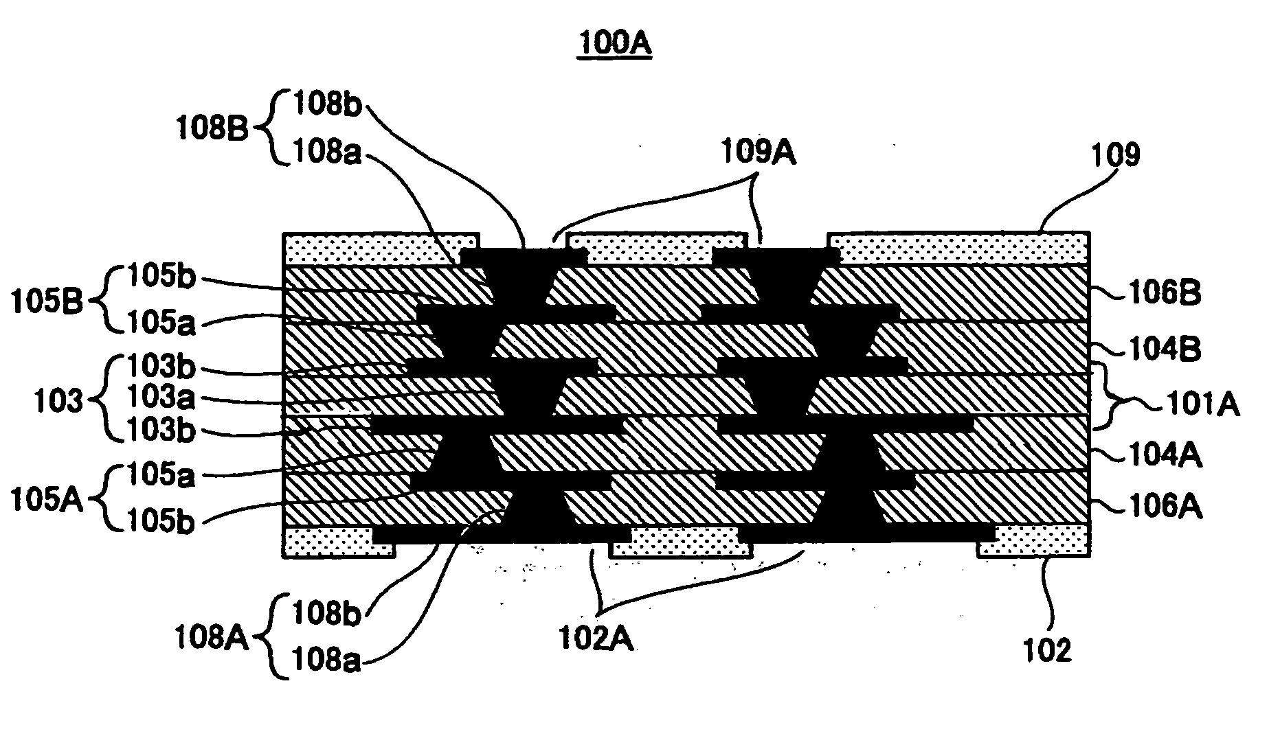
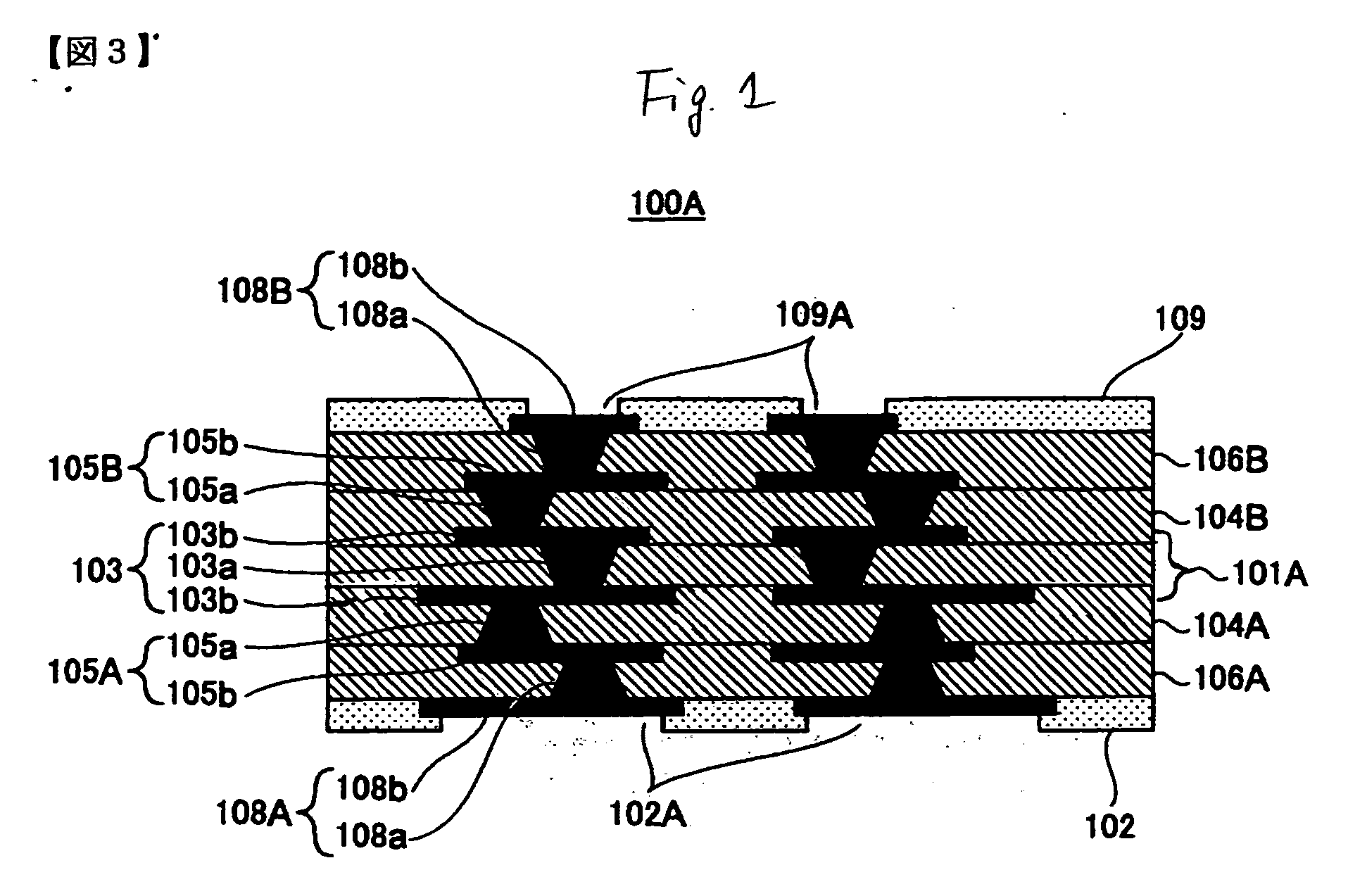
[0037]FIG. 1 shows a multilayered wiring substrate 100A according to the invention. As shown in this figure, in this embodiment, the explanation will be made as to a six-layer structure as an example of the multilayered wiring substrate 100A. However, the invention is not limited to the six-layer structure and can be widely applied to multilayered wiring substrate having various numbers of layers.

[0038] In brief, the multilayered wiring substrate 100A is configured by laminating a core layer 101A, first insulation layers 104A, 104B, wiring layers 105A, 105B, second insulation layers 106A, 106B and wiring layers 108A, 108B. A solder resist 102 is formed on the lower surface of the second insulation layer 106A and a solder resist 109 is formed on the upper surface of the second insulation layer 106B.

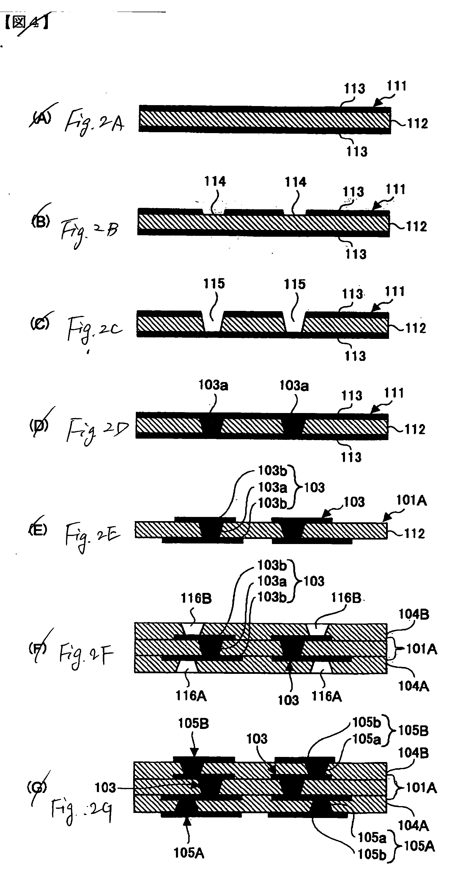
[0039] As shown in FIG. 2E, the core layer 101A is configured by an insulation material 112 and a wiring layer 103. The insulation material 112 is formed by epoxy build-up resin with the ...

second embodiment

[0072] The multilayered wiring substrate 100B shown in FIGS. 3 and 4 is characterized in that reinforcing portions 120 as well as the wiring layers 103 are formed at the insulation material 112 constituting the core layer 101B.

[0073] Since the reinforcing portions 120 are formed by the copper foils 113 (see FIG. 2A), the reinforcing portions can be formed simultaneously with the forming of the pattern wiring portions 103b. Further, the disposing positions of the reinforcing portions 120 are set at positions other than the preset forming positions of the pattern wiring portions 103b. Thus, the pattern wiring portions 103b are not influenced by the forming of the reinforcing portions 120. According to this configuration, since the reinforcing portions 120 are formed by using portions where the pattern wiring portions 103b are not formed, the mechanical intensity of the core layer 101B can be enhanced and so the multilayered wiring substrate 100B can be realized which has a high relia...

third embodiment

[0074] On the other hand, the multilayered wiring substrate 100C shown in FIGS. 5 and 6 is characterized in that plane-shaped wirings (so-called an all over pattern) as well as the wiring layers 103 are formed at the insulation material 112 constituting the core layer 101C. Although this embodiment shows an example that the plane-shaped wirings are formed as ground layers 122, the plane-shaped wirings may be formed as power source layers and, alternatively, may be configured as the mixture of the ground layers and the power source layers.

[0075] Since the ground layers 122 are also formed by the copper foils 113, the ground layers can be formed simultaneously with the forming of the pattern wiring portions 103b. Further, the disposing positions of the ground layers 122 are set at positions other than the preset forming positions of the pattern wiring portions 103b. Thus, the pattern wiring portions 103b are not influenced by the forming of the ground layers 122.

[0076] According to ...


PUM


Abstract

In a multilayered wiring substrate in which insulation layers 104A, 106A, wiring layers 105A, 108A and insulation layers 104B, 106B, wiring layers 105B, 108B are laminated on both side surfaces of a core layer 101A, respectively, the core layer 101A is constituted by insulation material 112 having no reinforcing member and copper foils 113 (pattern wiring portions 103b) formed on the both side surfaces of the insulation material 112.

Description

TECHNICAL FIELD [0001] The present disclosure relates to a multilayered wiring substrate and a manufacturing method thereof and, in particular, to a multilayered wiring substrate provided with a reinforcing means for preventing war page and a manufacturing method thereof RELATED ART [0002] At present, the high performance and the miniaturization of electronic devices using semiconductor devices such as semiconductor chips have been proceeded. According to such the proceeding, the semiconductor devices are also intended to be manufactured with a high density thereby to attempt the increase of the number of pins and the miniaturization. A multilayered wiring substrate utilizing the build-up method is provided as a substrate capable of mounting such the semiconductor device realizing the increase of the number of pins and the miniaturization. [0003] This kind of the multilayered wiring substrate is configured in a manner that a reinforcing member such as a glass cloth copper laminated ...

Claims


Application Information

Patent Timeline
Patent Type & Authority Applications(United States)
IPC IPC(8): H01L23/52
CPCH01L21/4857H01L23/49822H01L23/49894H01L23/552H01L23/66H05K3/0035H05K3/4602H01L2924/0002H05K2201/0394H05K2201/09563H05K2203/0554H05K2203/1572H01L2924/00
Inventor NAKAMURA, JUNICHI
Owner SHINKO ELECTRIC IND CO LTD
Why Eureka
Try Eureka