Plasma processing apparatus and method of suppressing abnormal discharge therein

a processing apparatus and plasma technology, applied in the direction of electrical apparatus, electrical discharge tubes, basic electric elements, etc., can solve the problems of destroying the workpiece itself, temporarily suspending the manufacturing process, replacing the defective workpiece, etc., to reduce the increase in the cost of manufacture and suppress the occurrence of abnormal discharge in plasma

Active Publication Date: 2007-03-15
RENESAS ELECTRONICS CORP
View PDF10 Cites 22 Cited by
  • Summary
  • Abstract
  • Description
  • Claims
  • Application Information

AI Technical Summary

Benefits of technology

[0018] In accordance with the present invention, the occurrence of abnormal discharge in plasma can be suppressed by controlling plasma based upon a detected foresee signal. Control of the plasma can be carried out by controlling a voltage for electrostatic adsorption, as a result of which abnormal discharge can be suppressed before it occurs. Alternatively, ESC leakage current c

Problems solved by technology

Accordingly, even if abnormal discharge of plasma is detected by the techniques disclosed in Patent Documents 1 and 2, contaminants will already have become attached to the workpiece owing to the abnormal discharge and the workpiece itself may be destroyed.
This makes it nece

Method used


Image

  • Plasma processing apparatus and method of suppressing abnormal discharge therein
  • Plasma processing apparatus and method of suppressing abnormal discharge therein
  • Plasma processing apparatus and method of suppressing abnormal discharge therein

Examples


first embodiment

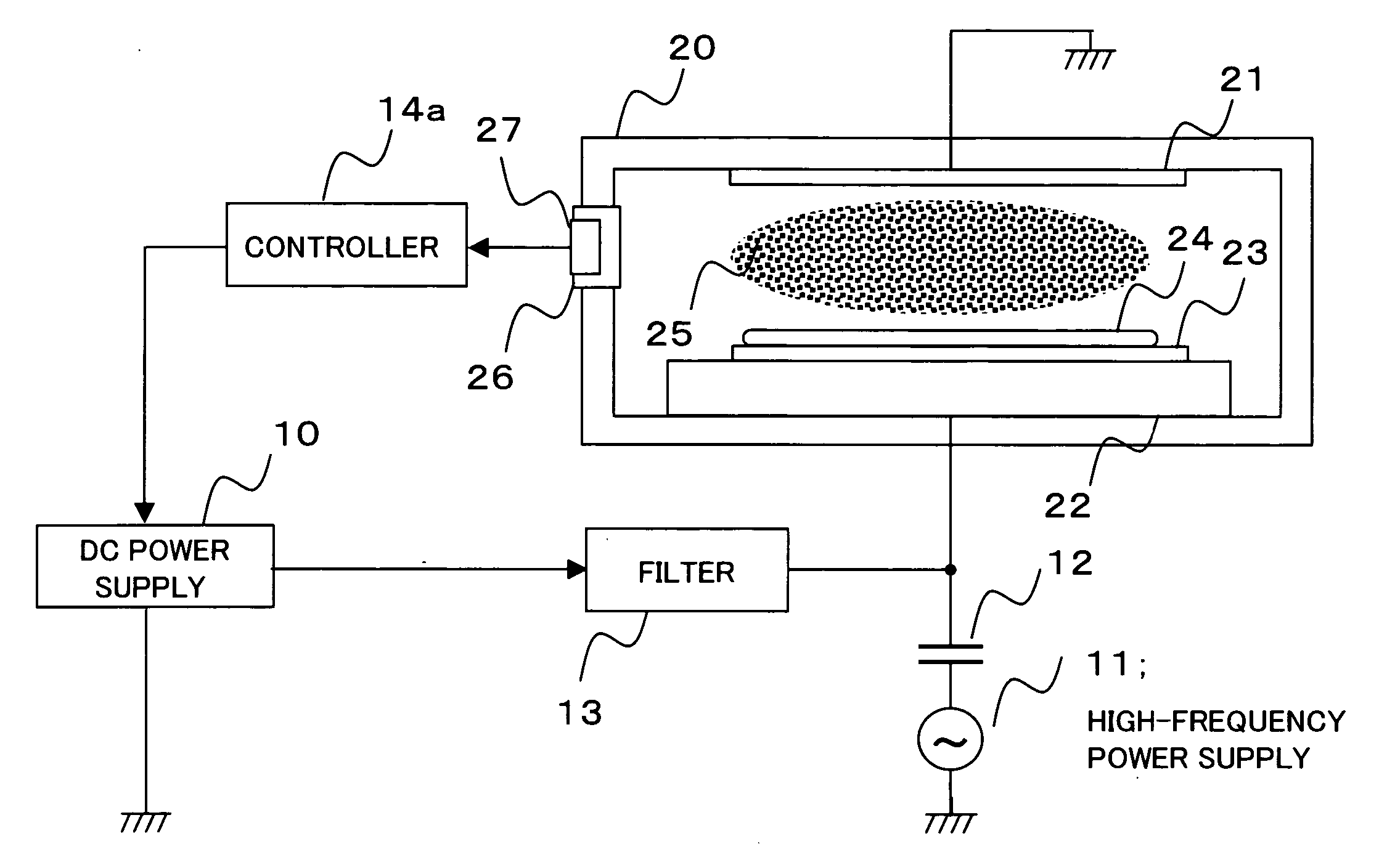
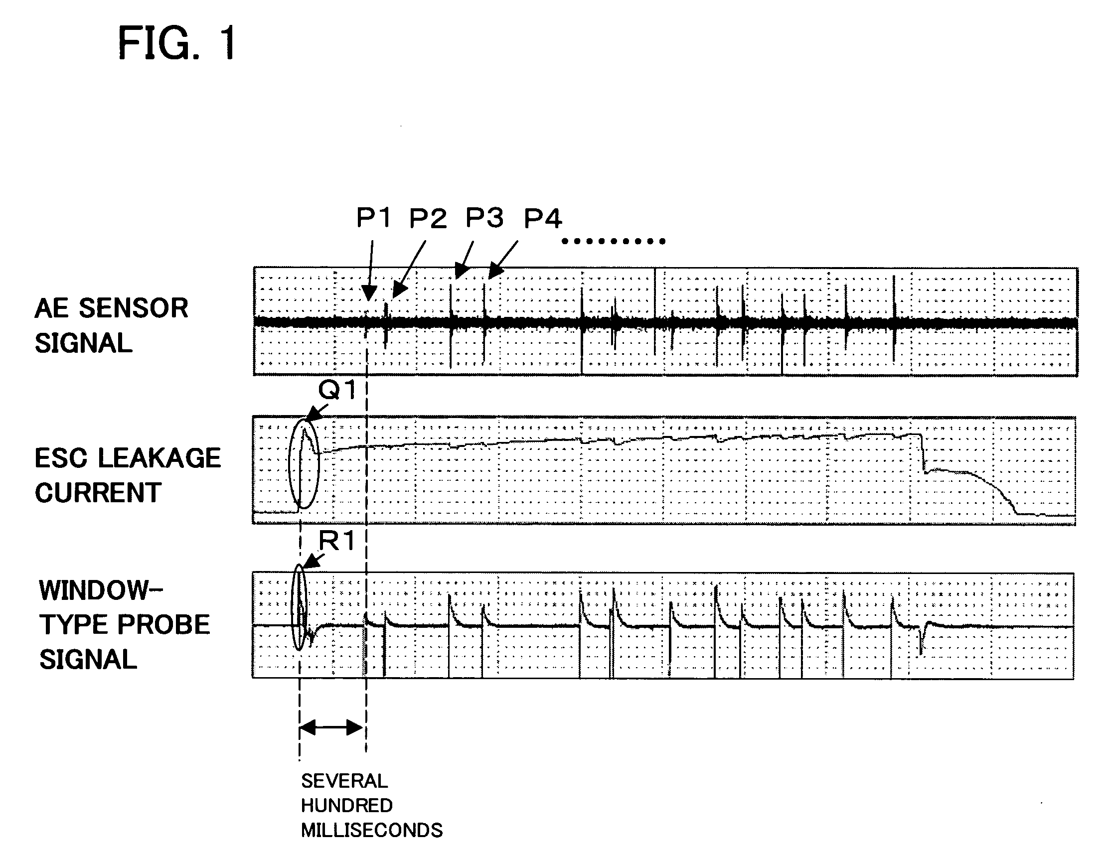
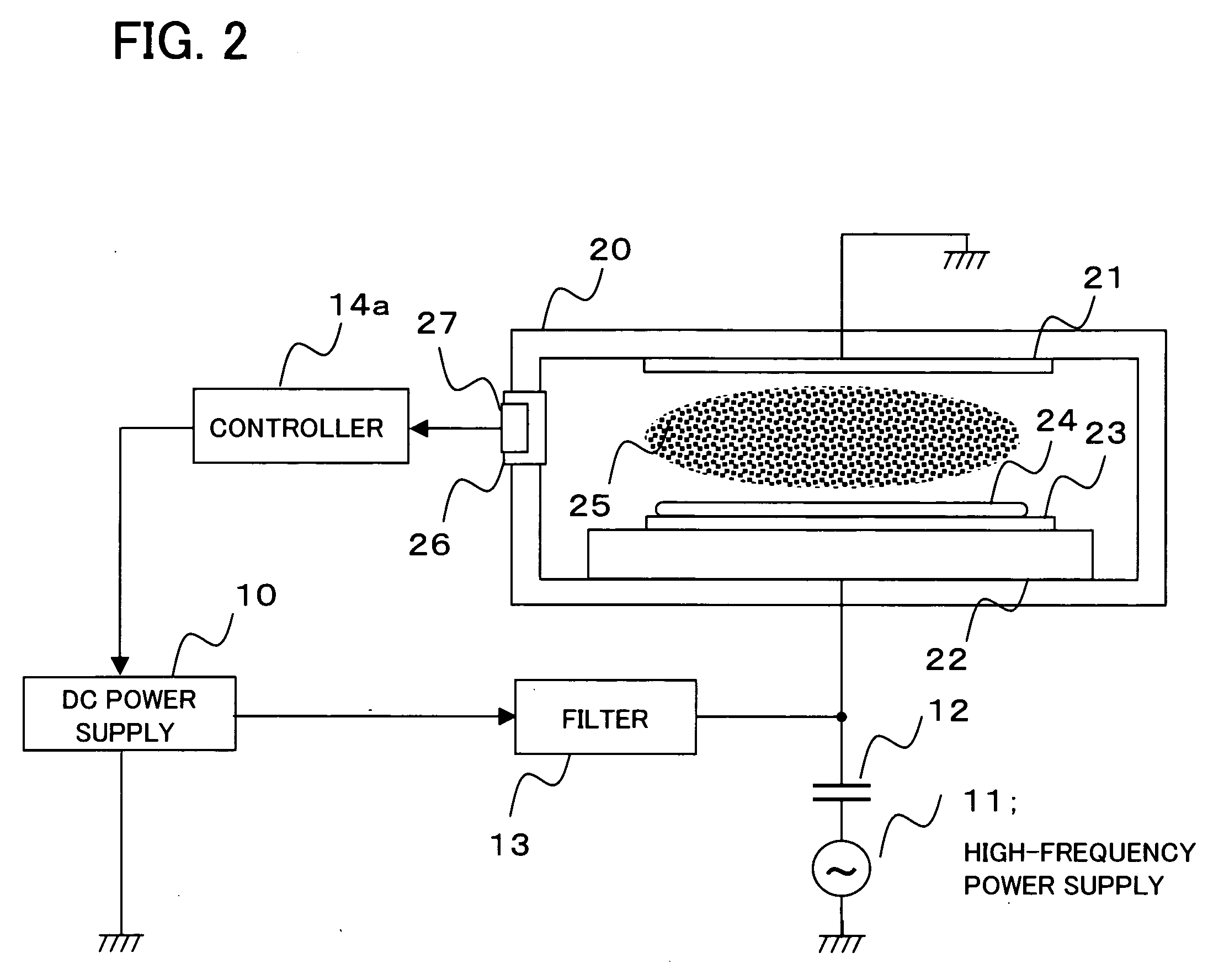
[0035]FIG. 2 is a block diagram illustrating the structure of a plasma processing apparatus according to a first embodiment of the present invention. As illustrated in FIG. 2, the plasma processing apparatus includes a DC power supply 10, a high-frequency power supply 11, a capacitor 12, a filter 13, a controller (control unit) 14a and a chamber 20. Further, the chamber 20 has an upper electrode 21, a lower electrode 22, an insulating film 23 and a window (view port) 26. A workpiece 24 to be processed, such as a semiconductor substrate, is placed on the insulating film 23.

[0036] The DC power supply 10 generates an electrostatic adsorption voltage of from several hundred to several thousand volts and supplies the voltage to the lower electrode 22 via the filter 13 as a high-voltage DC voltage (ESC potential). The lower electrode 22 is a constituent of an electrostatic chuck that holds the semiconductor substrate, etc., by electrostatic adsorption force. Provided on the lower electro...

second embodiment

[0048]FIG. 4 is a block diagram illustrating the structure of a plasma processing apparatus according to a second embodiment of the present invention. Components in FIG. 4 identical with those shown in FIG. 2 are designated by like reference characters and need not be described again. The plasma processing apparatus of FIG. 4 has a controller 14b and a current detector 15 instead of the controller 14a and window-potential detector 27, respectively, of the embodiment in FIG. 2. Abnormal discharge is foreseen based on a deleted signal of the current detector 15.

[0049] The current detector 15 is inserted between the DC power supply 10 and the filter 13 and detects the current (ESC current) supplied from the DC power supply 10 to the lower electrode 22. The controller 14b determines whether the ESC current lies within a prescribed range and, if the ESC current is outside the prescribed range, controls the DC power supply 10 so as to diminish the absolute value of the electrostatic adso...

third embodiment

[0057]FIG. 6 is a block diagram illustrating the structure of a plasma processing apparatus according to a third embodiment of the present invention. Components in FIG. 6 identical with those shown in FIG. 2 are designated by like reference characters and need not be described again. The plasma processing apparatus of FIG. 6 has a controller 14c instead of the controller 14a of the embodiment in FIG. 2. On the basis of a foresee signal in the controller 14c, the high-frequency power that is output by a high-frequency power supply 11a is controlled. More specifically, control is exercised so as to lower the high-frequency power in order to suppress abnormal discharge. In other words, lowering the high-frequency power also is equivalent to exercising control so as to reduce the absolute value of the electrostatic adsorption voltage, in the sense that the ESC leakage current is controlled. Accordingly, by exercising control so as to reduce high-frequency power when the signal represent...


PUM


Abstract

In a plasma processing apparatus having an electrostatic chuck for holding a semiconductor wafer by an electrostatic adsorption force and a DC power supply for applying an electrostatic adsorption voltage to the electrostatic chuck, abnormal discharge in plasma is suppressed by providing the apparatus with a signal detector that detects a foresee signal that foresees occurrence of abnormal discharge in plasma, and a controller that controls ESC leakage current based upon the foresee signal. If the foresee signal is outside a prescribed range, control is exercised so as to reduce the absolute value of the electrostatic adsorption voltage, thereby suppressing the occurrence of an abnormal discharge.

Description

FIELD OF THE INVENTION [0001] This invention relates to a plasma processing apparatus and to a method of suppressing abnormal discharge in this apparatus. More particularly, the invention relates to a processing apparatus in which a workpiece to be processed is held by an electrostatic chuck and the workpiece is processed using a high-frequency, high-voltage plasma discharge, and to a method of suppressing abnormal discharge produced in this processing apparatus. BACKGROUND OF THE INVENTION [0002] A plasma processing apparatus for processing the surface of a semiconductor substrate or the like using a plasma discharge is employed widely in the field of semiconductor manufacture. In a plasma processing apparatus, a workpiece to be processed such as a semiconductor substrate is subjected to plasma processing by producing a plasma across two electrodes (an electrode to which high-frequency power is applied and an opposing electrode to which a constant voltage is applied) provided insid...

Claims


Application Information

Patent Timeline
IPC IPC(8): H01T23/00
CPCH01L21/6833H01J2237/0206
Inventor ITO, NATSUKOYASAKA, MITSUOUESUGI, FUMIHIKOITAGAKI, YOUSUKE
Owner RENESAS ELECTRONICS CORP
Why Eureka
Try Eureka