Lateral double-diffused field effect transistor and integrated circuit having same

a field effect transistor and dual-diffused technology, applied in transistors, semiconductor devices, electrical equipment, etc., can solve the problems of increasing chip size and manufacturing costs, inability to increase breakdown voltage, etc., and achieve the effect of reducing manufacturing steps and reducing manufacturing costs

Inactive Publication Date: 2007-03-22
SHARP KK
View PDF3 Cites 24 Cited by
  • Summary
  • Abstract
  • Description
  • Claims
  • Application Information

AI Technical Summary

Benefits of technology

[0011] An object of the present invention is to provide a lateral double-diffused field effect transistor with high breakdown voltage and low on-resistance.

Problems solved by technology

The on-resistance of the MOS transistor is in close relationship with its size, that is, the larger size can reduce the on-resistance, although this causes increase in chip size and manufacturing costs.
This causes a problem of inability in increasing the breakdown voltage.

Method used


Image

  • Lateral double-diffused field effect transistor and integrated circuit having same
  • Lateral double-diffused field effect transistor and integrated circuit having same
  • Lateral double-diffused field effect transistor and integrated circuit having same

Examples


Embodiment Construction

[0056] The present invention is hereinbelow described in detail in conjunction with the embodiments with reference to the drawings.

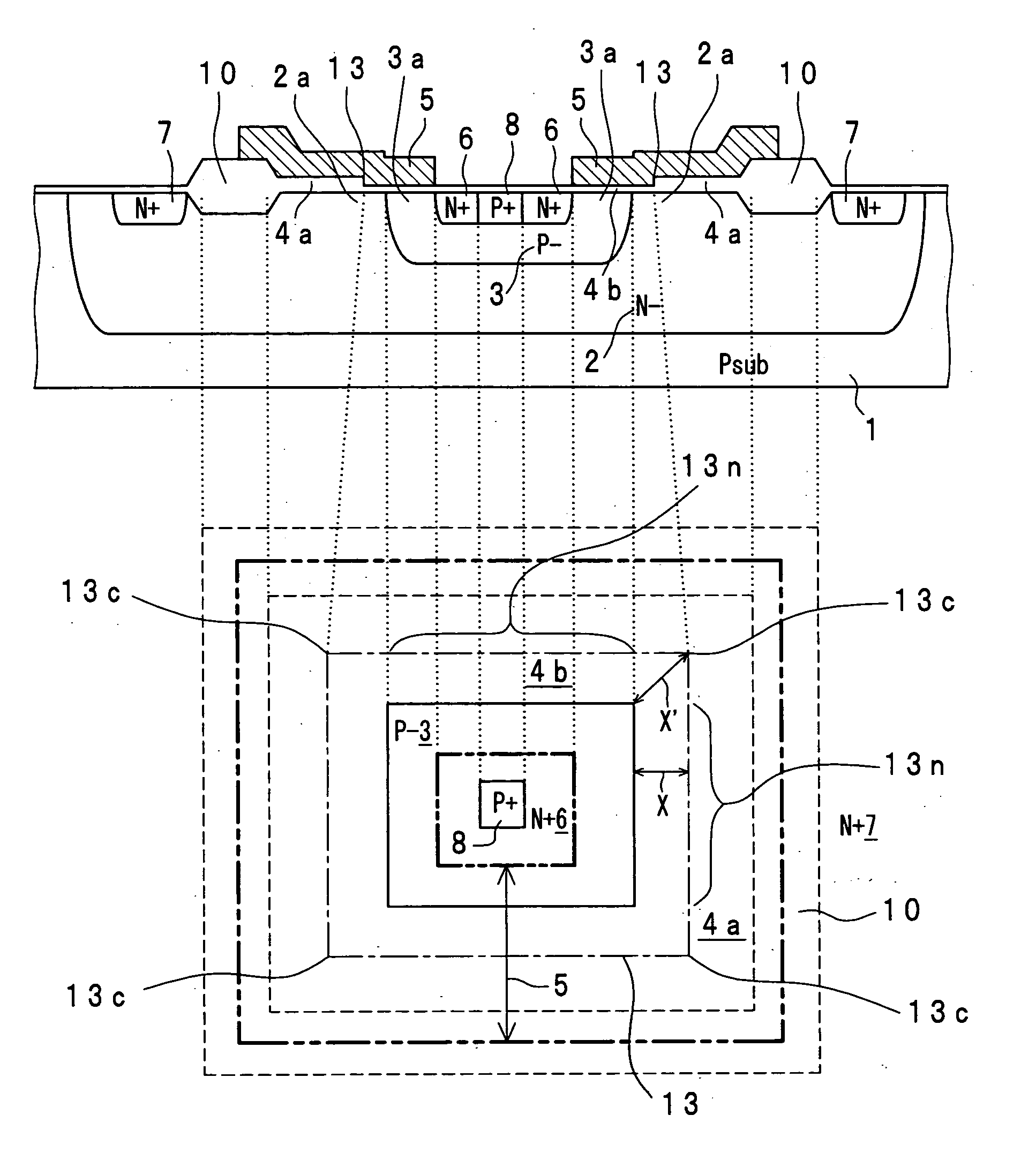
[0057] The upper half of FIG. 3A shows a cross sectional structure of a lateral double-diffused MOS transistor fundamental to the present invention, while the lower half of FIG. 3A shows a plan pattern layout of the lateral double-diffused MOS transistor corresponding to the cross sectional structure.

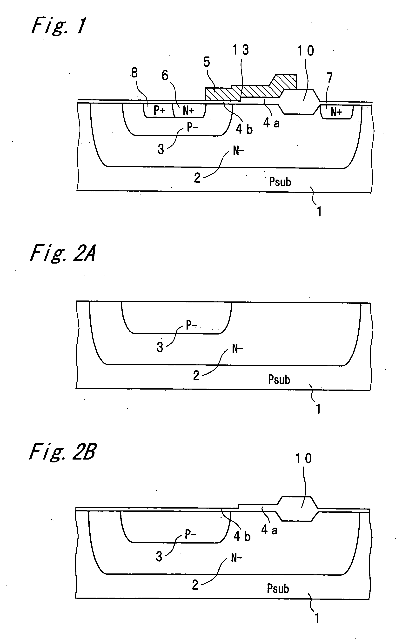
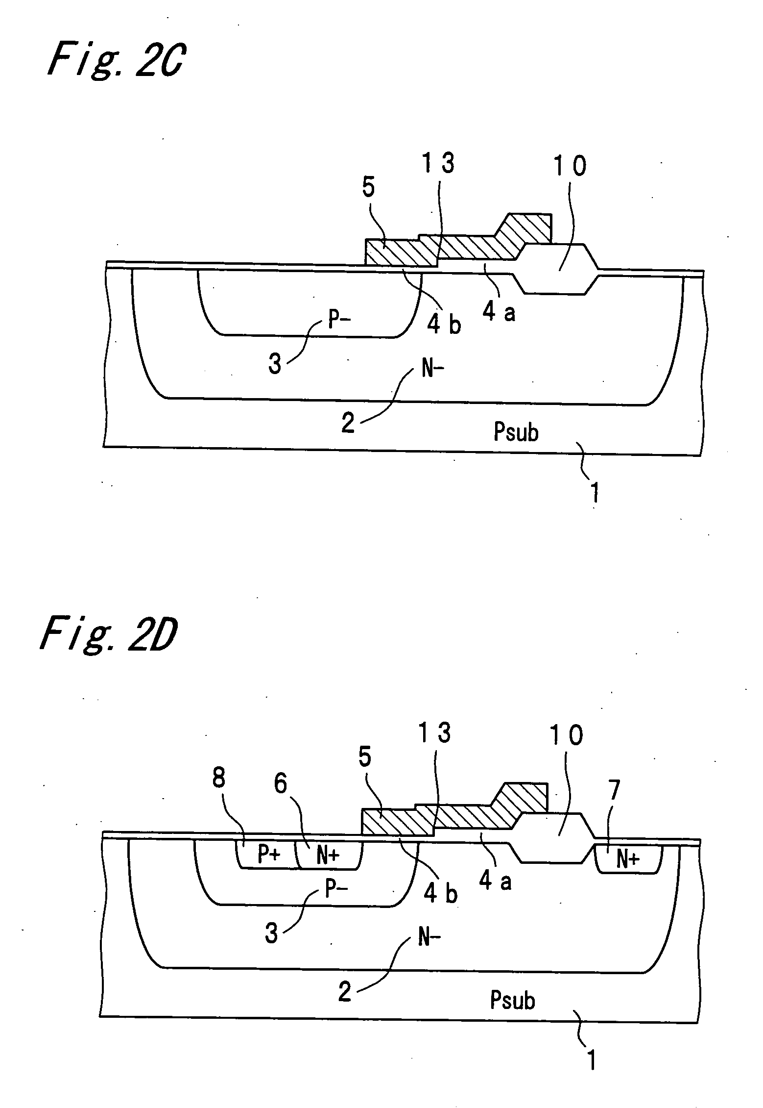
[0058] The lateral double-diffused MOS transistor, which is an N-channel MOS transistor, is formed on a lightly-doped N-well diffusion layer 2 formed with N-type impurity being diffused on the surface of a P-type substrate 1. The lateral double-diffused MOS transistor comprises a P-body diffusion layer 3 formed on the surface of the N-well diffusion layer 2 with use of a rectangular pattern, an N+ source diffusion layer 6 formed in the central section in the P-body diffusion layer 3 with use of a rectangular pattern, and an N+ drain diffusion layer 7 forme...


PUM


Abstract

In a lateral double-diffused field effect transistor of the present invention, a gate insulating film includes a first gate insulating film covering a source diffusion layer up to a region beyond the pattern of a body diffusion layer and a second gate insulating film having a film thickness larger than that of the first gate insulating film and covering a region closer to a drain diffusion layer than the region covered by the first gate insulating film. A boundary between the first gate insulating film and the second gate insulating film is composed of a straight portion parallel to a side of the pattern of the body diffusion layer and a corner portion surrounding an vertex of the pattern of the body diffusion layer from a distance. A distance between the vertex of the pattern of the body diffusion layer and the corner portion of the boundary is equal to or smaller than a distance between the side of the pattern of the body diffusion layer and the straight portion of the boundary.

Description

[0001] This Nonprovisional application claims priority under 35 U.S.C. §119(a) on Patent Application No. 2005-251475 filed in Japan on Aug. 31, 2005, the entire contents of which are hereby incorporated by reference. BACKGROUND OF THE INVENTION [0002] The present invention relates to a lateral double-diffused field effect transistor, and typically relates to a lateral double-diffused MOS transistor. [0003] The present invention also relates to an integrated circuit having such a lateral double-diffused field effect transistor. [0004] In recent years, with progress of multifunctional electronic equipment, semiconductor devices used therefor are diversified and the semiconductor devices are required to have high breakdown voltage, high power, downsizing, and low power consumption. In order to accomplish the lower power consumption, transistors with low on-resistance are necessary. [0005]FIG. 6 shows a cross sectional structure of a general lateral double-diffused MOS transistor (see, ...

Claims


Application Information

Patent Timeline
Patent Type & Authority Applications(United States)
IPC IPC(8): H01L29/94H01L29/76H01L31/00
CPCH01L29/0696H01L29/0886H01L29/7816H01L29/66681H01L29/42368H01L29/735
Inventor TAKIMOTO, TAKAHIRONAKAMURA, HIROKIFUKUSHIMA, TOSHIHIKO
Owner SHARP KK
Why Eureka
Try Eureka