

Impedance adjusting circuit and impedance adjusting method
- Summary
- Abstract
- Description
- Claims
- Application Information
AI Technical Summary
Benefits of technology
Problems solved by technology
Method used
Image

Examples
Embodiment Construction
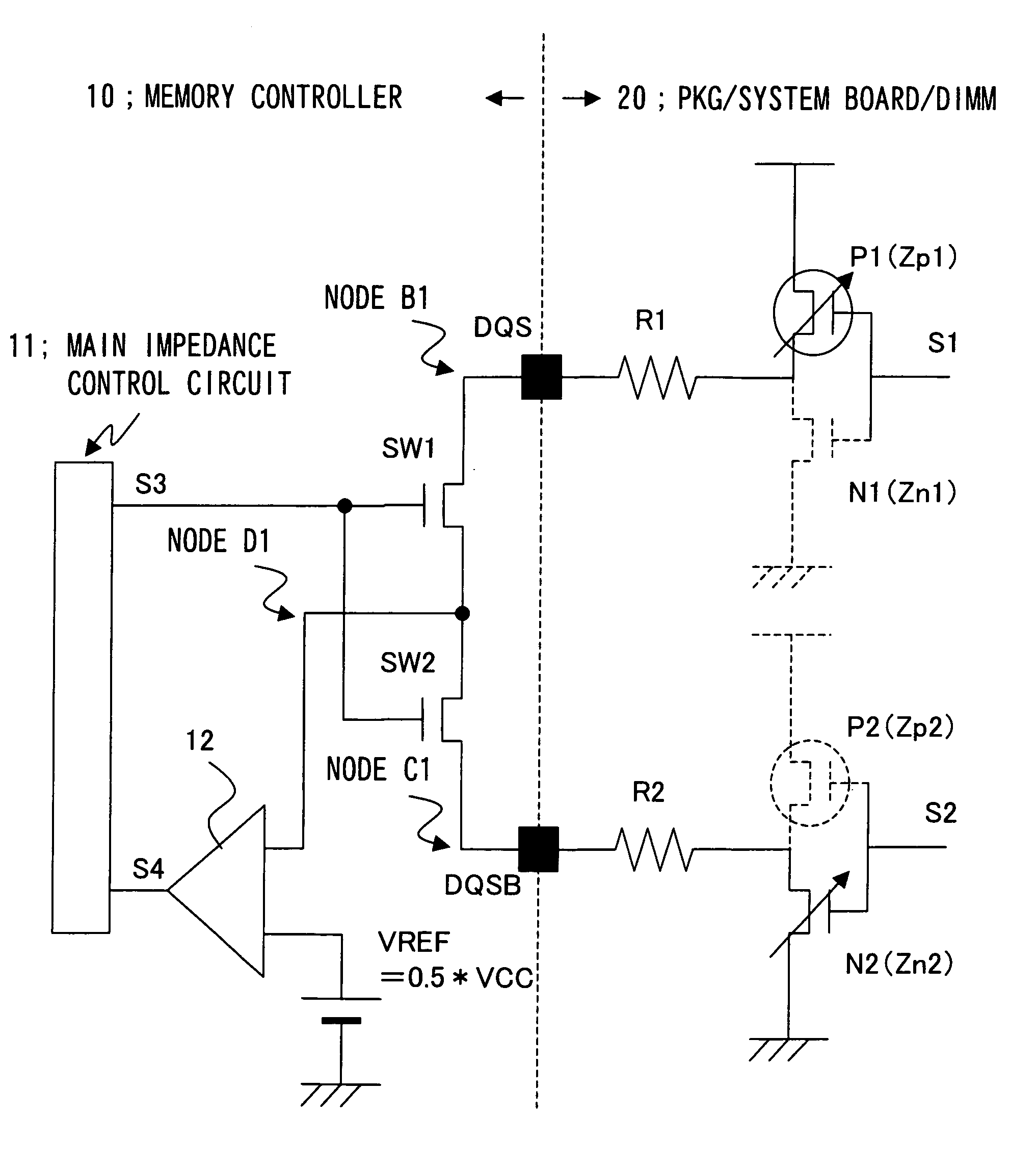
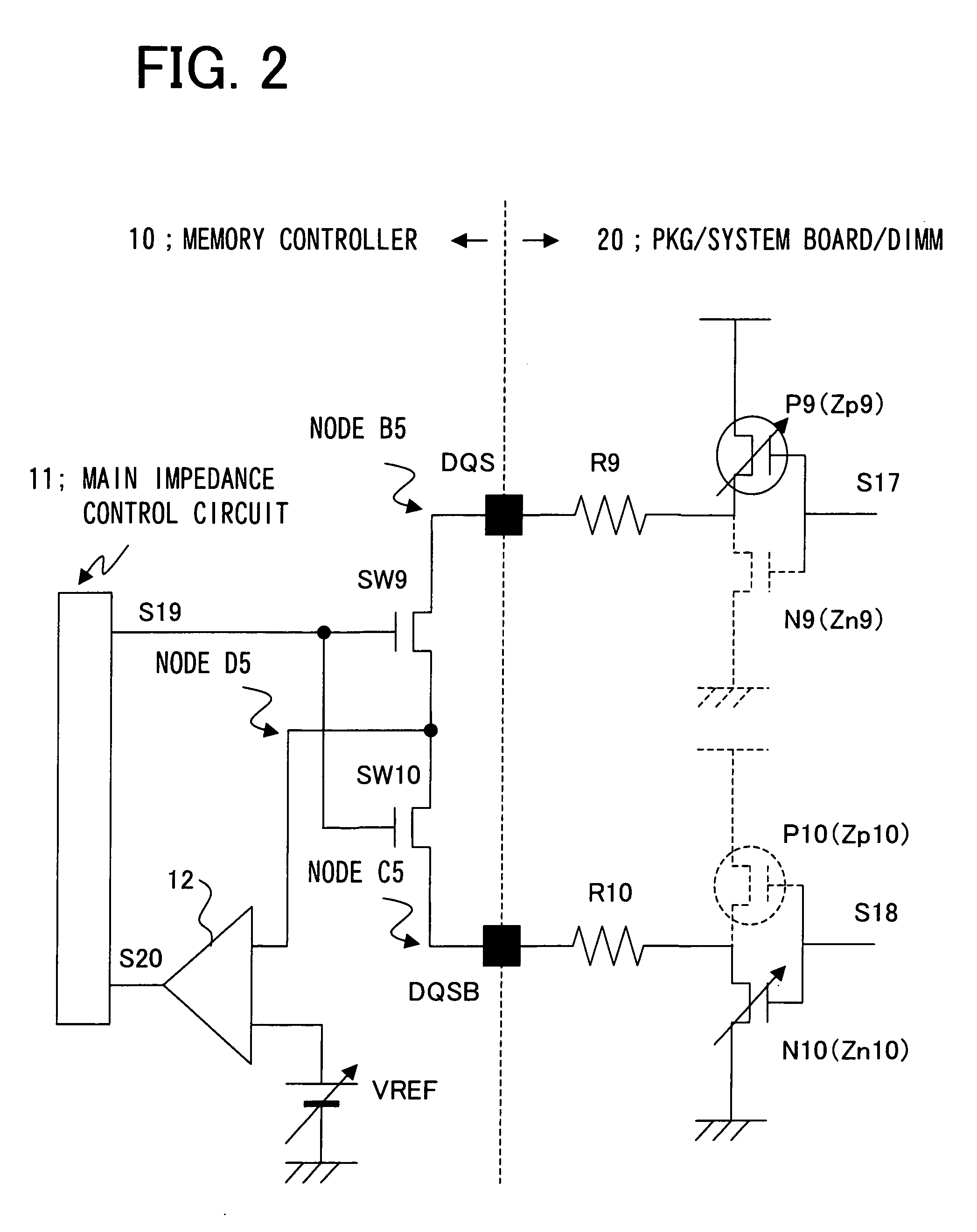
[0059] The preferred embodiments of the present invention with be described with reference to appended drawings. In the present invention, by comparing impedances of a pull-up output buffer and a pull-down output buffer using complementary output signals such as differential strobe signals (DQS, DQSB) for data control from a DDR2 memory side, using an OD impedance adjusting function of a DDR2 memory, relative impedance adjustment is made. Since the relative impedance adjustment is made, series resistance components on the package / system board / DIMM are compensated and prohibited from influencing the impedance adjustment.
[0060] Generally, lengths of wiring for important signals that determine an operating speed of a system, such as a data signal (DQ) and the differential strobe signals (DQS, DQSB) for data control, are made equal on the package / system board / DIMM so that delays thereof are equal.
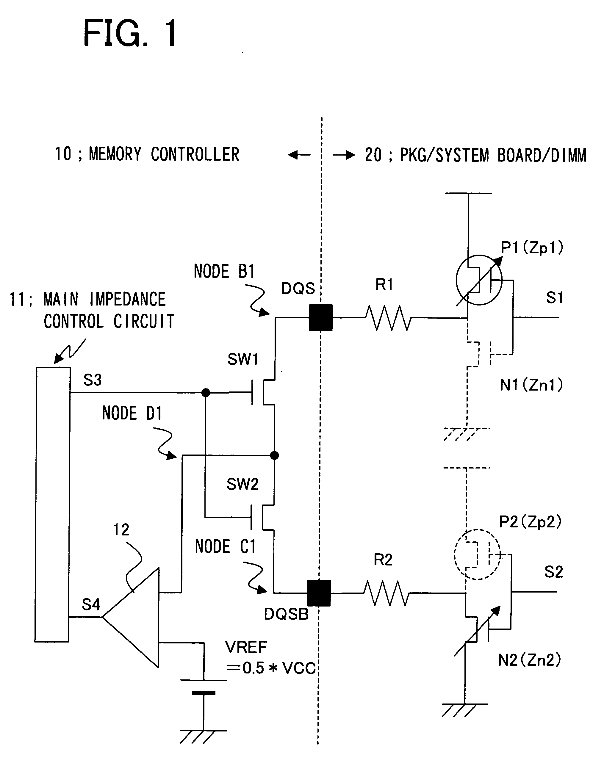
[0061]FIG. 1 is a diagram showing a configuration of an embodiment of the present inventi...
PUM
 Abstract
Description
Claims
Application Information