Image sensing device and manufacture method thereof

a technology of image sensing device and manufacturing method, which is applied in the field of optoelectronic devices, can solve the problems of image sensor design problems, inability to dispose of every micro lens, and inability to achieve the effect of simple and efficient disposal, and achieve the effect of increasing the refraction of incident ligh

Inactive Publication Date: 2007-03-29
VISERA TECH CO LTD
View PDF5 Cites 12 Cited by
  • Summary
  • Abstract
  • Description
  • Claims
  • Application Information

AI Technical Summary

Benefits of technology

[0031] Preferably, the image sensing device further includes an intermediate layer separating the micro lens and the micro prism for increasing the refraction of the incident light.

Problems solved by technology

No matter it is the CCD or CMOS image sensor being used, the optical crosstalk effect is always a problem to the designer of the image sensor.
However, since four photodiodes 122 in each pixel set are grouped together, the layout of the micro lens array 124 is changed to an non-uniform decenter layout, which may result in the overlapped layout of the micro lens array 124, as shown in FIG. 13.
Since it is very complicated and inefficient to dispose every micro lenses, the micro lens layer 42 are categorized into several groups according to their distances from the center of the sensor chip center.
However, such an image sensor still has the problem relating to the photo crosstalk effect and the brightness difference.
Base on the above, the conventional image sensors still have the problems in eliminating the crosstalk effect and the brightness difference.

Method used


Image

  • Image sensing device and manufacture method thereof
  • Image sensing device and manufacture method thereof
  • Image sensing device and manufacture method thereof

Examples


Embodiment Construction

[0070] The present invention will now be described more specifically with reference to the following embodiments. It should to be noted that the following descriptions of preferred embodiments of this invention are presented herein for purposes of illustration and description only; it is not intended to be exhaustive or to be limited to the precise form disclosed.

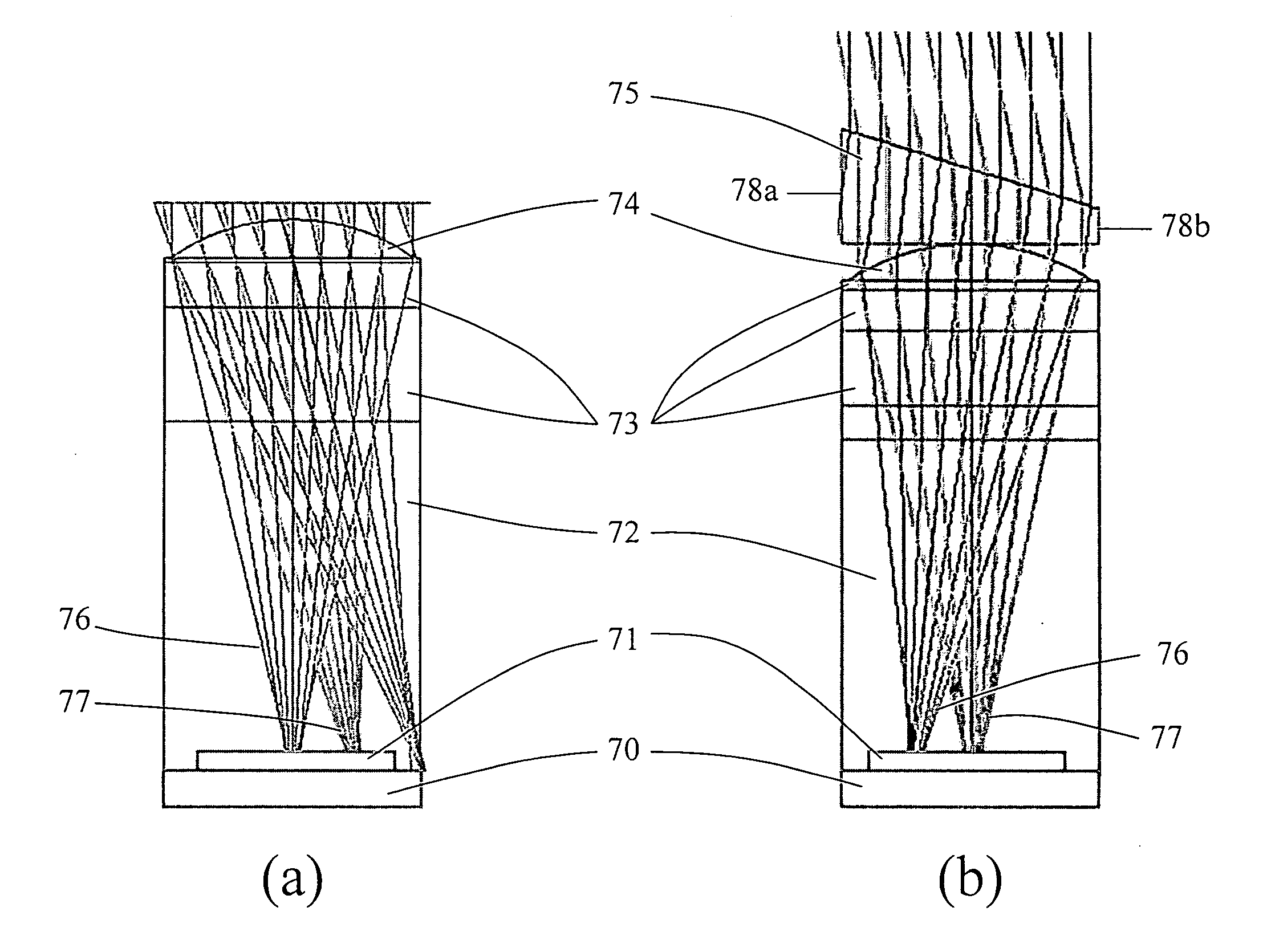
[0071] In an image sensing device according to the present invention, a micro prism array is incorporated thereinto, so that the light with a larger chief ray angle, which is an angle between the incident light and the vertical line, can be adjusted to a light with a smaller incident angle for decreasing the optical crosstalk effect among adjacent pixels of the image sensing device.

[0072] Please refer to FIG. 6, which schematically explains the working principle of a micro prism. The micro prism 62 has an inclined angle α, which is defined by the angle between the normal 64a of the entrance plane 64 and the vertical line ...


PUM


Abstract

An image sensing device for receiving an incident light having an incident angle and photo signals formed thereby is provided. The image sensing device includes a micro prism and a micro lens for adjusting the incident angle and converging the incident light, respectively, a photo sensor for converting the photo signals into electronic signals, and an IC stacking layer for processing the electronic signals.

Description

FIELD OF THE INVENTION [0001] The present invention refers to an optoelectronic device, in particular to a structure and arrangement of an image sensing device. BACKGROUND OF THE INVENTION [0002] Structure of Image Sensor [0003] As the applications of the optoelectonic device become more and more popular, the demands for the image sensing device increase rapidly. In general, typical image sensors can be categorized into two main parts, which are the charge coupled device (CCD) and the complementary metal-oxide semiconductor (CMOS). [0004] An image sensor is used for recording a change of a photo signal formed by an image and converting the photo signal into an electronic signal. After recording and processing the electronic signal, a digital image is generated for further outputting or recording. In general, the image sensor is formed by a plurality of photo sensing devices, which are either CCD elements or COMS elements. [0005] A CCD image sensor is formed by a capacitor array havi...

Claims


Application Information

Patent Timeline
Patent Type & Authority Applications(United States)
IPC IPC(8): H01L27/00H01L27/14H01L31/0232H04N5/335H04N5/369
CPCH01L27/14603H01L27/14621H01L27/14685H01L27/14627H01L27/14625
Inventor LEE, HSIAO-WEN
Owner VISERA TECH CO LTD
Why Eureka
Try Eureka