Bi-directional read/program non-volatile floating gate memory array, and method of formation
- Summary
- Abstract
- Description
- Claims
- Application Information
AI Technical Summary
Problems solved by technology
Method used
Image

Examples
Embodiment Construction
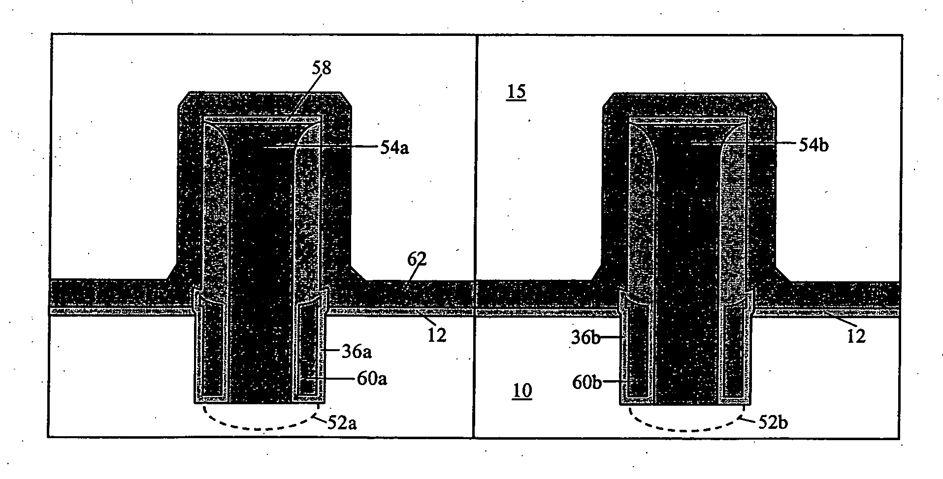
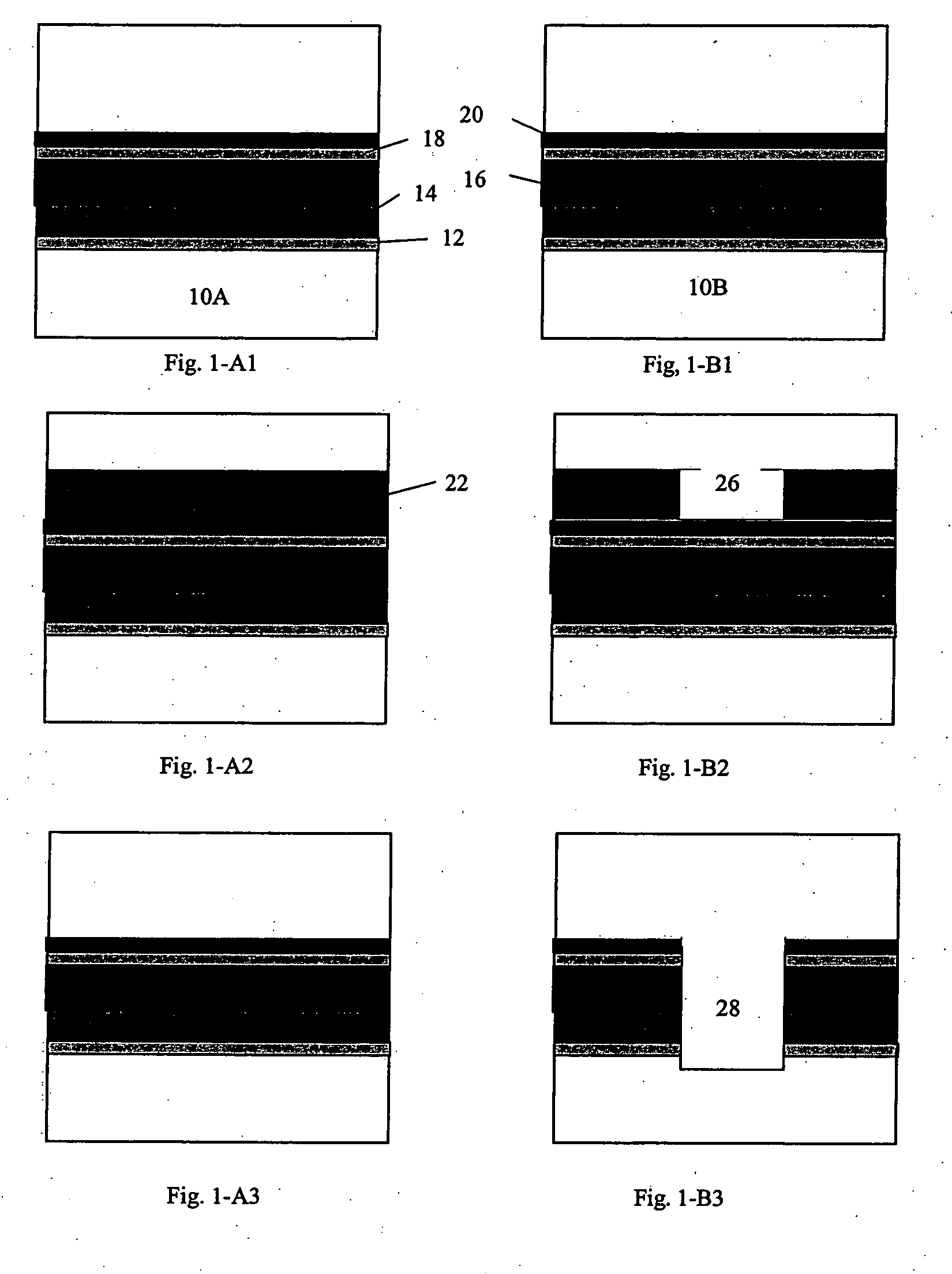
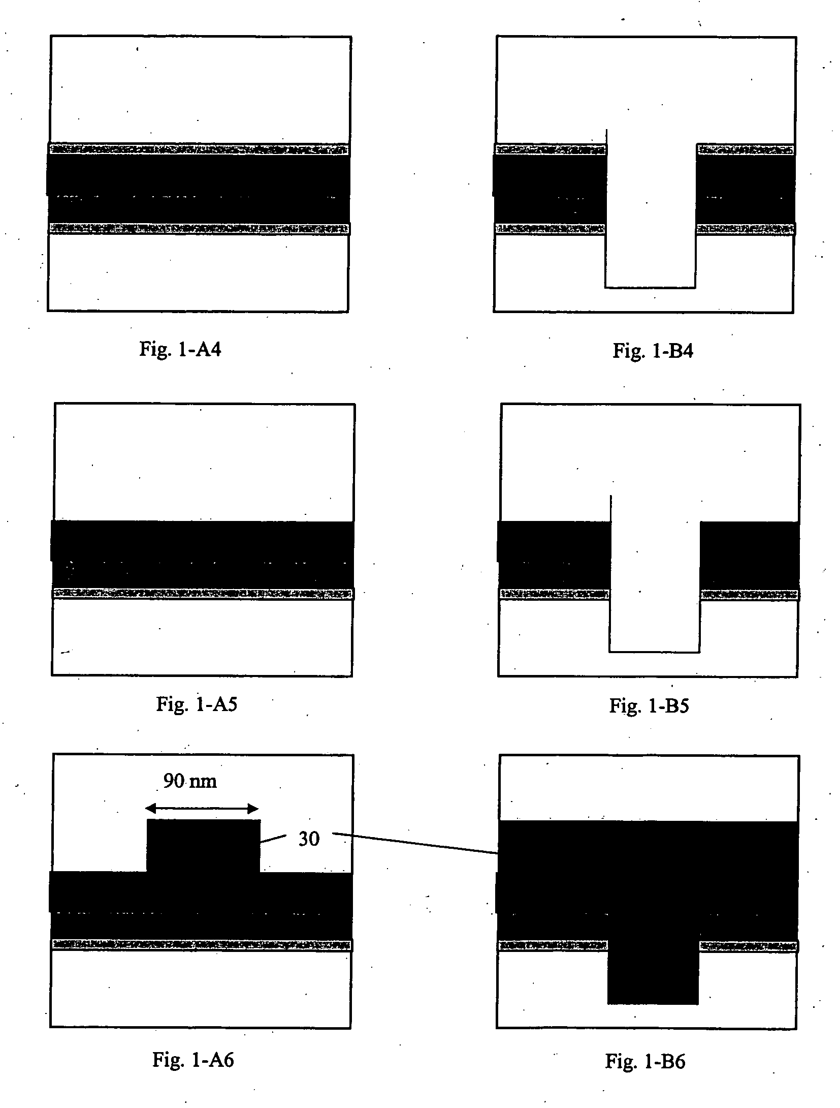
[0011] The present invention relates to an array of non-volatile memory cells, without any isolation between rows of adjacent active regions, and a method of making thereof, which is illustrated in FIGS. 2A to 2K. However, as is well known in the art, an array of non-volatile memory cells is typically integrated with peripheral circuits on an integrated circuit. Further, typically, isolation regions must be formed in the peripheral circuit portion of an integrated circuit memory device. Thus, before discussing the method of manufacturing the array of the present invention, a discussion will be made as to the methods for the formation of the isolation regions in the peripheral circuits.
[0012] The method begins with a semiconductor substrate 10, which is preferably of P type and is well known in the art. The thickness of the layers described below will depend upon the design rules and the process technology generation. What is described herein is for the 90 nm process. However, it wi...
PUM
 Abstract
Description
Claims
Application Information
PatSnap Eureka turns technology decisions into work you can execute. Powered by our Innovation Knowledge Graph, it runs expert workflows across engineering, life sciences, materials and intellectual property. Get your review-ready output in minutes.


