Method of forming bottom oxide for nitride flash memory

a technology of nitride flash memory and bottom oxide, which is applied in the direction of semiconductor devices, instruments, electrical appliances, etc., can solve the problems of severe degradation of device performance, adversely affecting the operating life, and non-volatile memory devices

Active Publication Date: 2007-03-29
MACRONIX INT CO LTD
View PDF5 Cites 93 Cited by
  • Summary
  • Abstract
  • Description
  • Claims
  • Application Information

AI Technical Summary

Problems solved by technology

However, a number of concerns exist regarding known non-volatile memory devices and methods for manufacturing.
For example, increases in interface trap densities (Dit) in a memory device may cause severe degradation of the device performance and adversely affect the operating life.
In some cases, high temperature baking may anneal the trap charge Qit, leading to equivalent Vt loss, which may be in the amount of Qit / Cono.
While high temperature baking may anneal interface traps, and annealing of interface traps may also contribute to Vt loss, which may result in data retention problems in a high temperature environment. FIG. 4 plots Vt versus time for a fresh device and a device that underwent 100,000 cycles at a temperature of 250° C. Experimental data showed that Vt loss was greater for the cycled device than for a fresh device in high temperatures.
Thus, a fresh non-volatile memory device with a large Dit is subject to a slower growth rate of Dit during cycling compared with a fresh device with a small Dit.
Also, a fresh device with a low quality of bottom oxide (BOX) could not properly retain data in high temperature environments.

Method used


Image

  • Method of forming bottom oxide for nitride flash memory
  • Method of forming bottom oxide for nitride flash memory
  • Method of forming bottom oxide for nitride flash memory

Examples


Embodiment Construction

[0026] Reference will now be made in detail to the exemplary embodiments of the invention, examples of which are illustrated in the accompanying drawings. Wherever possible, the same reference numbers will be used throughout the drawings to refer to the same.

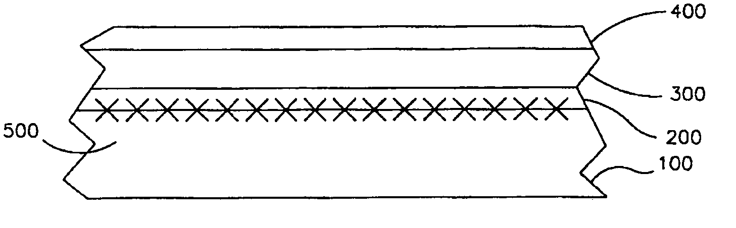
[0027] The following exemplary methods and devices overcome one or more disadvantages of prior devices methods of forming memory devices. According to one embodiment, a non-volatile memory device comprising a top oxide layer, a bottom oxide layer; and a middle layer of silicon nitride over a semiconductor substrate. The bottom oxide layer may have a hydrogen concentration of up to 5E19 cm−3 and an interface trap density of up to 5E11 cm−2 eV−1. In one particular example, the concentration of hydrogen may be between about 1E17 cm−3 and about 5E19 cm−3. In another example, the interface trap density may be between about 1E10 cm−2 eV−1 and about 5E11 cm−2 eV−1.

[0028]FIG. 12 shows a schematic diagram illustrating one example of a ...


PUM

PropertyMeasurementUnit
temperatureaaaaaaaaaa
energy levelaaaaaaaaaa
temperatureaaaaaaaaaa

Abstract

A non-volatile memory device on a semiconductor substrate may include a bottom oxide layer over the substrate, a middle layer of silicon nitride over the bottom oxide layer, and a top oxide layer over the middle layer. The bottom oxide layer may have a hydrogen concentration of up to 5E19 cm−3 and an interface trap density of up to 5E11 cm−2 eV−1. The three-layer structure may be a charge-trapping structure for the memory device, and the memory device may further include a gate over the structure and source and drain regions in the substrate.

Description

BACKGROUND OF THE INVENTION [0001] This disclosure relates generally to nonvolatile memory devices. More particularly, the present disclosure relates to nitride flash memory devices and methods for manufacture thereof. [0002] Nonvolatile memory devices may have various structural designs. FIG. 1 shows an example of a nonvolatile memory cell that is implemented in and on a substrate. A memory cell may comprise source and drain regions 10, as well as a channel 20 disposed between the source and drain regions. Overlying channel is a charge-trapping or ONO structure 25, which may comprise a charge-trapping nitride layer 30 (e.g. silicon nitride) disposed between two oxide layers 40 (e.g. silicon oxide). Each memory cell may further comprise a gate electrode 50 that overlies the charge trapping structure 25. The charge-trapping structure 25 and the gate electrode 50 may be isolated from other structures on the substrate, such as source and drain contacts by spacers 60 shown in FIG. 1. By...

Claims


Application Information

Patent Timeline
Patent Type & Authority Applications(United States)
IPC IPC(8): H01L29/792H01L21/471H01L21/8239
CPCG11C16/0466H01L29/513H01L21/28282H01L29/40117
Inventor SHIH, YEN-HAOLUE, HANG-TINGLAI, ERH-KUNHSIEH, KUANG YEU
Owner MACRONIX INT CO LTD
Why Eureka
Try Eureka